Flexible Packaging for Chip-on-Chip and Package-on-Package Technologies

a technology of chip-on-chip and packaging technology, applied in the field of integrated circuit packaging, can solve the problems affecting the operation of the chip-on-chip, and affecting the quality of the chip-on-chip, so as to achieve the effect of reducing the size of the packaging substra

Active Publication Date: 2010-09-16
APPLE INC
View PDF25 Cites 15 Cited by
  • Summary
  • Abstract
  • Description
  • Claims
  • Application Information

AI Technical Summary

Benefits of technology

[0008]In one embodiment, a packaging solution for an application integrated circuit (IC) and one or more other ICs is provided. The packaging solution may support both chip-on-chip packaging of the application IC (in flip-chip connection to a package substrate) and other ICs (in non-flip chip orientation). The packaging solution may also support package-on-package packaging of the application IC and the other ICs. The package substrate may include a first set o...

Problems solved by technology

Each packaging solution has associated risks as well.
Package-on-package technology carries more risk (e.g. in terms of parts that do not operate correctly and must be disposed of at manufacture, in terms of earlier failure due to defects not yet apparent in a newer technology, in terms of early failure of the ...

Method used


Image

  • Flexible Packaging for Chip-on-Chip and Package-on-Package Technologies
  • Flexible Packaging for Chip-on-Chip and Package-on-Package Technologies
  • Flexible Packaging for Chip-on-Chip and Package-on-Package Technologies

Examples


Embodiment Construction

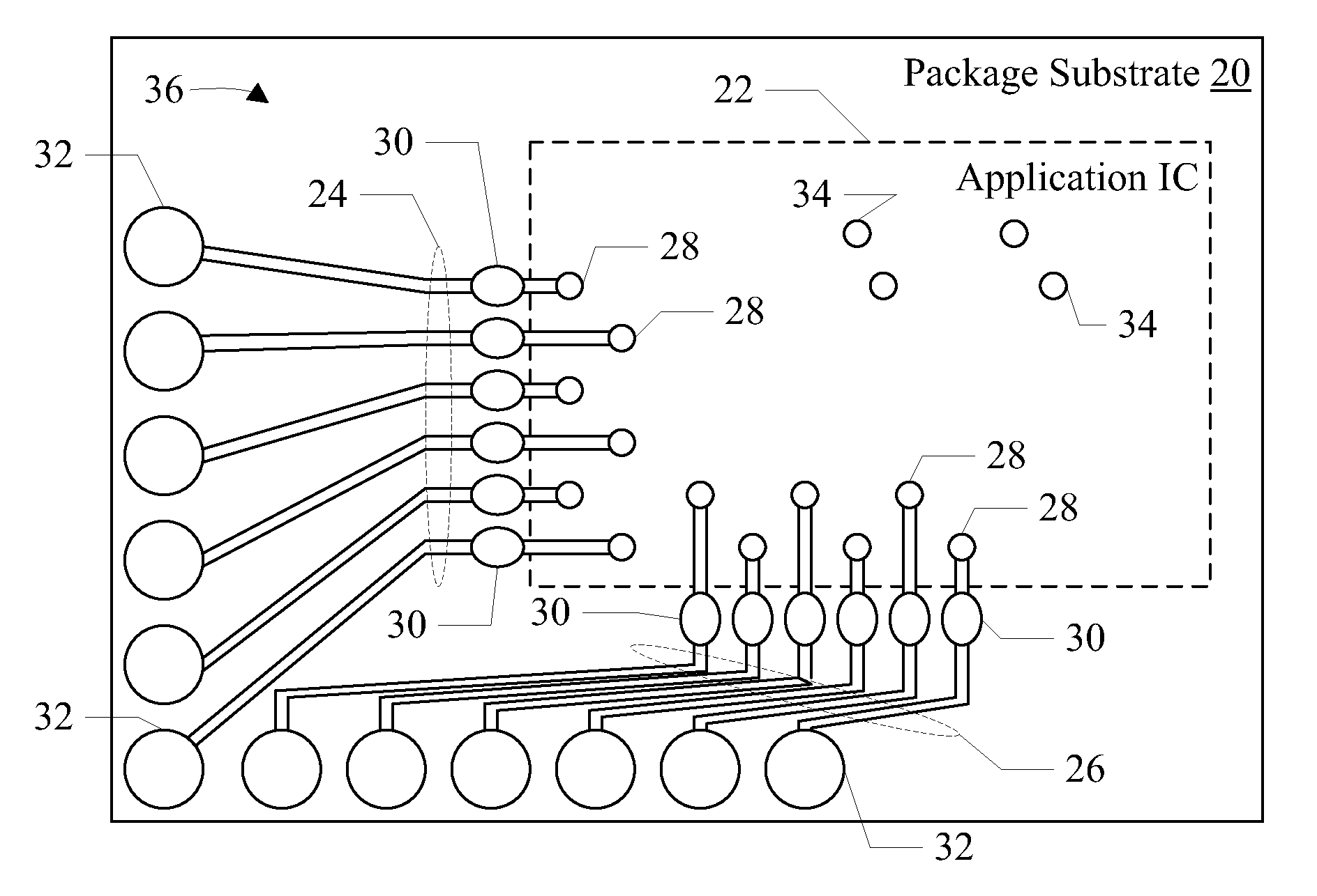
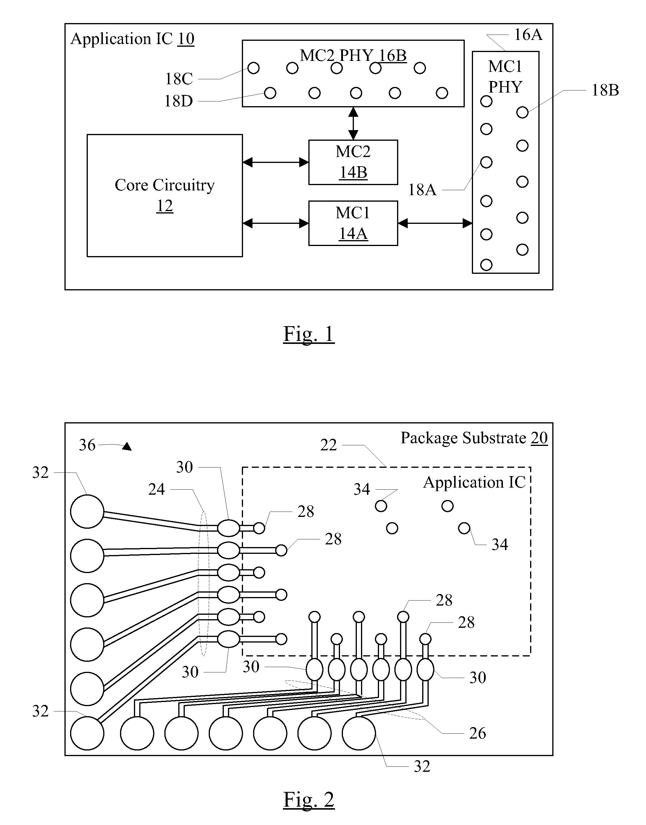
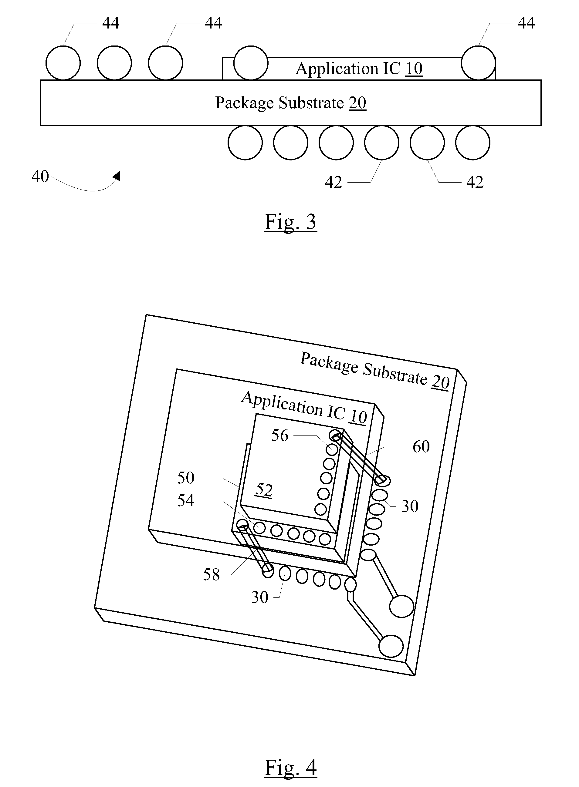
[0020]In one embodiment, a packaging solution may support chip-on-chip packaging and may also maintain support for package-on-package packaging for the same chips. The package-on-package implementation may be a proven technology (as compared to a chip-on-chip implementation), and thus its risk factor may be lower than the chip-on-chip implementation. The chip-on-chip implementation may have a higher risk factor, but may also reduce the size of the overall package. If the chip-on-chip implementation proves to be reliable, the support for the package-on-package solution may be removed and the package size may be reduced. On the other hand, if the chip-on-chip implementation proves unreliable, the same package may be used to package the integrated circuit at the bottom of the stack with separately-packaged instances of the other integrated circuits in a package-on-package solution. Accordingly, the packaging solution described herein may permit chip-on-chip packaging while offsetting t...


PUM


Abstract

In one embodiment, a packaging solution for an application integrated circuit (IC) and one or more other ICs is provided. The packaging solution may support both chip-on-chip packaging of the application IC (in flip-chip connection to a package substrate) and other ICs (in non-flip chip orientation), and package-on-package packaging of the application IC and the other ICs. The package substrate may include a first set of pads proximate to the application IC to support chip-on-chip connection to the other ICs. The pads may be connected to conductors that extend underneath the application IC, to connect to the application IC. A second set of pads may be connected to package pins for package-on-package solutions. If the chip-on-chip solution proves reliable, support for the package-on-package solution may be eliminated and the package substrate may be reduced in size.

Description

BACKGROUND[0001]1. Field of the Invention[0002]This invention is related to the field of integrated circuits and, more particularly, to packaging of integrated circuits.[0003]2. Description of the Related Art[0004]Integrated circuit chips are generally packaged to provide more convenient and reliable connection to other components such as a circuit board, to protect the integrated circuit from damage, etc. Originally, each integrated circuit chip was housed in its own package, which was soldered or otherwise electrically and physically connected to a circuit board to which other integrated circuits (each in their own packages) and other electronic components were also connected.[0005]More recently, package-on-package connections have been used to reduce the size of the device that includes the integrated circuits. In such cases, a first integrated circuit is packaged in a package that includes pins to connect to a circuit board and which also includes mounting points that match the ...

Claims


Application Information

Patent Timeline
IPC IPC(8): H01L23/48H01L23/522H01L21/50
CPCH01L22/32H01L23/49816H01L2924/07802H01L23/49838H01L23/50H01L24/05H01L24/16H01L24/48H01L25/0657H01L25/105H01L25/18H01L25/50H01L2224/13144H01L2224/1319H01L2224/32145H01L2224/48227H01L2225/0651H01L2225/06517H01L2225/06524H01L2225/06527H01L2225/06551H01L2225/06555H01L2225/06562H01L2225/06596H01L2924/0102H01L2924/01079H01L2924/14H01L2924/1433H01L2924/15173H01L2924/15311H01L2924/15312H01L2924/15313H01L2924/15192H01L2225/1023H01L2225/1058H01L24/24H01L24/82H01L2224/24225H01L2224/82101H01L2225/1005H01L2224/16225H01L2924/00H01L2224/0401H01L2924/00014H01L2224/45099H01L2224/45015H01L2924/207
Inventor VON KAENEL, VINCENT R.
Owner APPLE INC
Why Eureka
Try Eureka