

Io cell with multiple io ports and related techniques for layout area saving
a technology of layout area and io cell, which is applied in the direction of electrical apparatus, semiconductor devices, semiconductor/solid-state device details, etc., to achieve the effect of saving chip layout area, compact io cell arrangement and chip layout area saving
- Summary
- Abstract
- Description
- Claims
- Application Information
AI Technical Summary
Benefits of technology
Problems solved by technology
Method used
Image

Examples
Embodiment Construction
[0033]The present invention will now be described more specifically with reference to the following embodiments. It is to be noted that the following descriptions of preferred embodiments of this invention are presented herein for purpose of illustration and description only; it is not intended to be exhaustive or to be limited to the precise form disclosed.
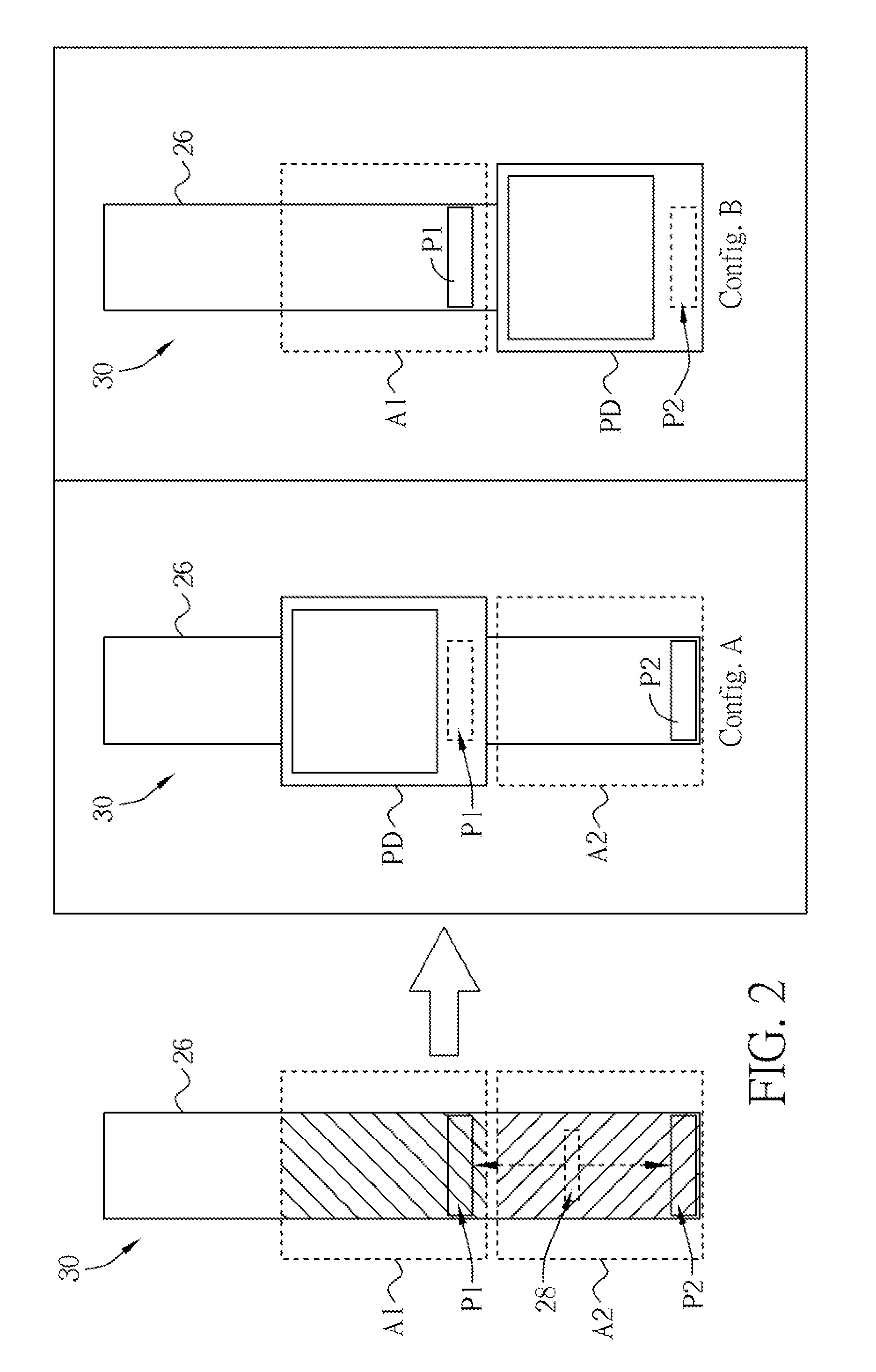
[0034]Please refer to FIG. 2 which illustrates an IO cell 30 according to an embodiment of the invention. Circuit layout of the IO cell 30 is contained in a main region 26, and the IO cell 30 has a plurality of IO ports; in the embodiment of FIG. 2, two IO ports P1 and P2 are shown as an example of the invention. IO ports P1 and P2 locate in the main region 26 and correspond to a same IO pin 28, such that both these two IO ports P1 and P2 can transmit signal of the IO pin 28. The IO ports P1 and P2 respectively correspond to predetermined regions A1 and A2, each of the predetermined regions A1 and A2 can be selectively used to co...
PUM
 Abstract
Description
Claims
Application Information