
Method and apparatus for electrostatic discharge protection having a stable breakdown voltage and low snapback voltage

a technology of electrostatic discharge protection and breakdown voltage, applied in the direction of electrical apparatus, semiconductor devices, semiconductor/solid-state device details, etc., can solve the problems of esd damage to integrated circuits in computers, communication equipment, etc., and achieve the effect of reducing initial current, high breakdown voltage and saving device layout area

Active Publication Date: 2009-10-13
DELPHI TECH IP LTD
View PDF1 Cites 4 Cited by
  • Summary
  • Abstract
  • Description
  • Claims
  • Application Information

AI Technical Summary

Benefits of technology

The solution provides stable and low-voltage snapback protection, allowing for scalable device design, saving layout area, and maintaining stability over repeated ESD strikes, while enabling precise control over ESD properties without significant redesign.

Problems solved by technology

ESD can damage integrated circuits in computers, communication equipment, and countless other types of electronic equipment.
These conventional devices provide ESD protection between two terminals, and are typically constructed to snapback at a particular voltage and current, which may be too high for satisfactory ESD protection, and which is dictated by the doping levels of the diffusions that break down.
The ESD protection devices conventionally available generally suffer from lack of control of the breakdown voltage and critical voltage, due to physical design parameters.
Since conventional ESD protection fails to handle sufficiently low snapback voltages and currents, a snapback voltage requirement for a particular device may require having to design a new device.

Method used


Image

  • Method and apparatus for electrostatic discharge protection having a stable breakdown voltage and low snapback voltage
  • Method and apparatus for electrostatic discharge protection having a stable breakdown voltage and low snapback voltage
  • Method and apparatus for electrostatic discharge protection having a stable breakdown voltage and low snapback voltage

Examples


Embodiment Construction

[0019]Exemplary embodiments are described with reference to specific configurations. Those of ordinary skill in the art will appreciate that various changes and modifications can be made while remaining within the scope of the appended claims. Additionally, well-known elements, devices, components, methods, process steps and the like may not be set forth in detail in order to avoid obscuring the invention. Further, unless indicated to the contrary, the numerical values set forth in the following specification and claims are approximations that may vary depending upon the desired characteristics sought to be obtained by the present invention.

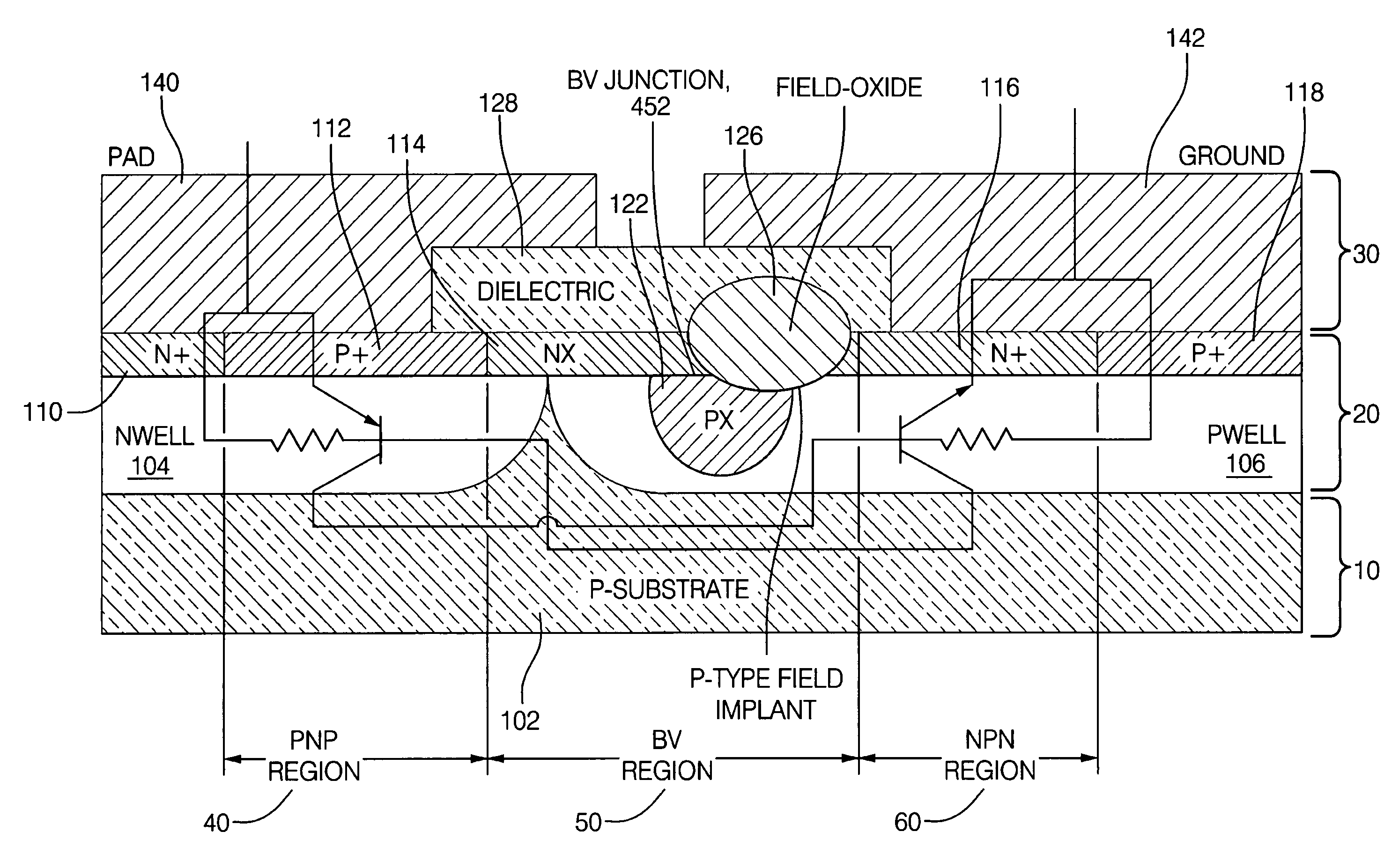
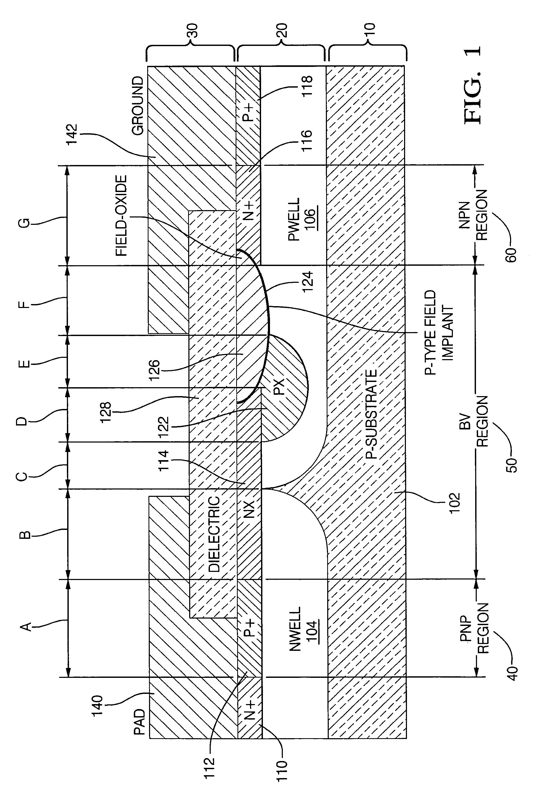
[0020]A silicon controlled rectifiers (SCR) system and method is described herein for protecting low voltage circuit input and outputs against electrostatic discharge (ESD), such as may be used in an integrated circuit. The present invention snaps back at a lower initial voltage, wherein the breakdown voltage can be tightly controlled and remains...


PUM


Abstract

Electrostatic discharge (ESD) protection is provided for an integrated circuit. Snap back from a lower initial critical voltage and critical current is provided, as compared to contemporary designs. A dynamic region having doped regions is formed on a substrate, interconnects contacting the dynamic region. The dynamic region includes an Nwell region, a Pwell region and shallow diffusions, defining a PNP region, an NPN region and a voltage Breakdown region. In an aspect, the Nwell region includes a first N+ contact, a first P+ contact and an N+ doped enhancement, while the Pwell region includes a second N+ contact, a second P+ contact and a P+ doped enhancement. The N+ doped enhancement contacts the P+ doped enhancement forming the breakdown voltage region therebetween, in one case forming a buried breakdown voltage junction. Independent control is provided over breakdown voltage, NPN critical voltage, NPN critical current and PNP critical current, by varying doping levels, widths and positioning of various doping regions.

Description

FIELD OF THE INVENTION[0001]The invention relates generally to a semiconductor integrated circuit, and more particularly to electrostatic discharge protection having a highly stable and low breakdown voltage, critical voltage and snapback voltage, which are independently controlled.BACKGROUND OF THE INVENTION[0002]Numerous electronic circuits require protection from damage due to electrostatic discharge (ESD) caused by rapid discharge of static electricity from one conductor to another having a different potential. ESD can damage integrated circuits in computers, communication equipment, and countless other types of electronic equipment. Semiconductor circuits and components built to provide ESD protection are conventionally implemented using components such as Shockley diodes, thyristors, latches, silicon controlled rectifiers (SCR) and metal gate field oxide (MGFO) devices. These conventional devices provide ESD protection between two terminals, and are typically constructed to sn...

Claims


Application Information

Patent Timeline
Patent Type & Authority Patents(United States)
IPC IPC(8): H01L29/72
CPCH01L27/0262H01L29/7436H01L2924/0002H01L2924/00
Inventor GLENN, JACK L.
Owner DELPHI TECH IP LTD
Learn More