Semiconductor device

a technology of semiconductor devices and pixel electrodes, applied in the direction of semiconductor devices, electrical equipment, transistors, etc., can solve the problems of limited tft development and the affect of the aperture ratio of pixel electrodes, and achieve the effect of increasing the layout area of other components, increasing the aperture ratio, and small layout area

Active Publication Date: 2013-09-05
E INK HLDG INC
View PDF4 Cites 4 Cited by
  • Summary
  • Abstract
  • Description
  • Claims
  • Application Information

AI Technical Summary

Benefits of technology

[0020]Based on the description above, the semiconductor device of the invention is designed to save the layout area of the component layer (including the metal layer, the insulating layer, the semiconductor layer, the drain and the source) on the surface of the substrate. Hence, the semiconductor device of the invention is advantageous not only in occupying a smaller layout area to allow increasing the layout area of other components on the substrate, but also in increasing the aperture ratio.

Problems solved by technology

Under a limited area of panel condition however, the increasing dimension of the TFT certainly squeezes the space for deposing other circuit wires or components and meanwhile, the aperture ratio of pixel electrode is affected.
As a result, the development of TFT is limited.

Method used


Image

  • Semiconductor device
  • Semiconductor device
  • Semiconductor device

Examples


Embodiment Construction

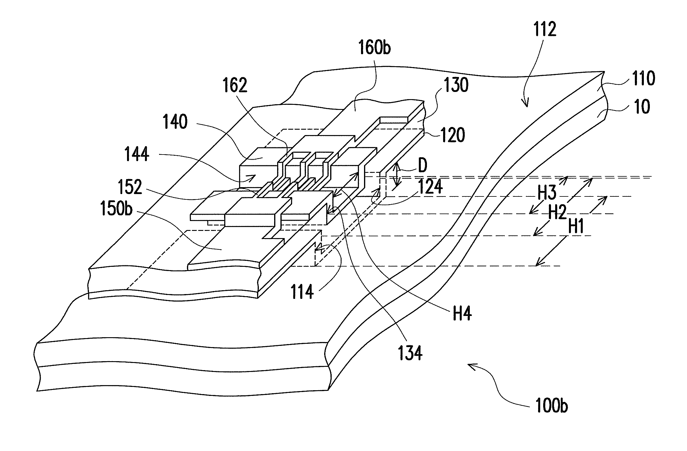
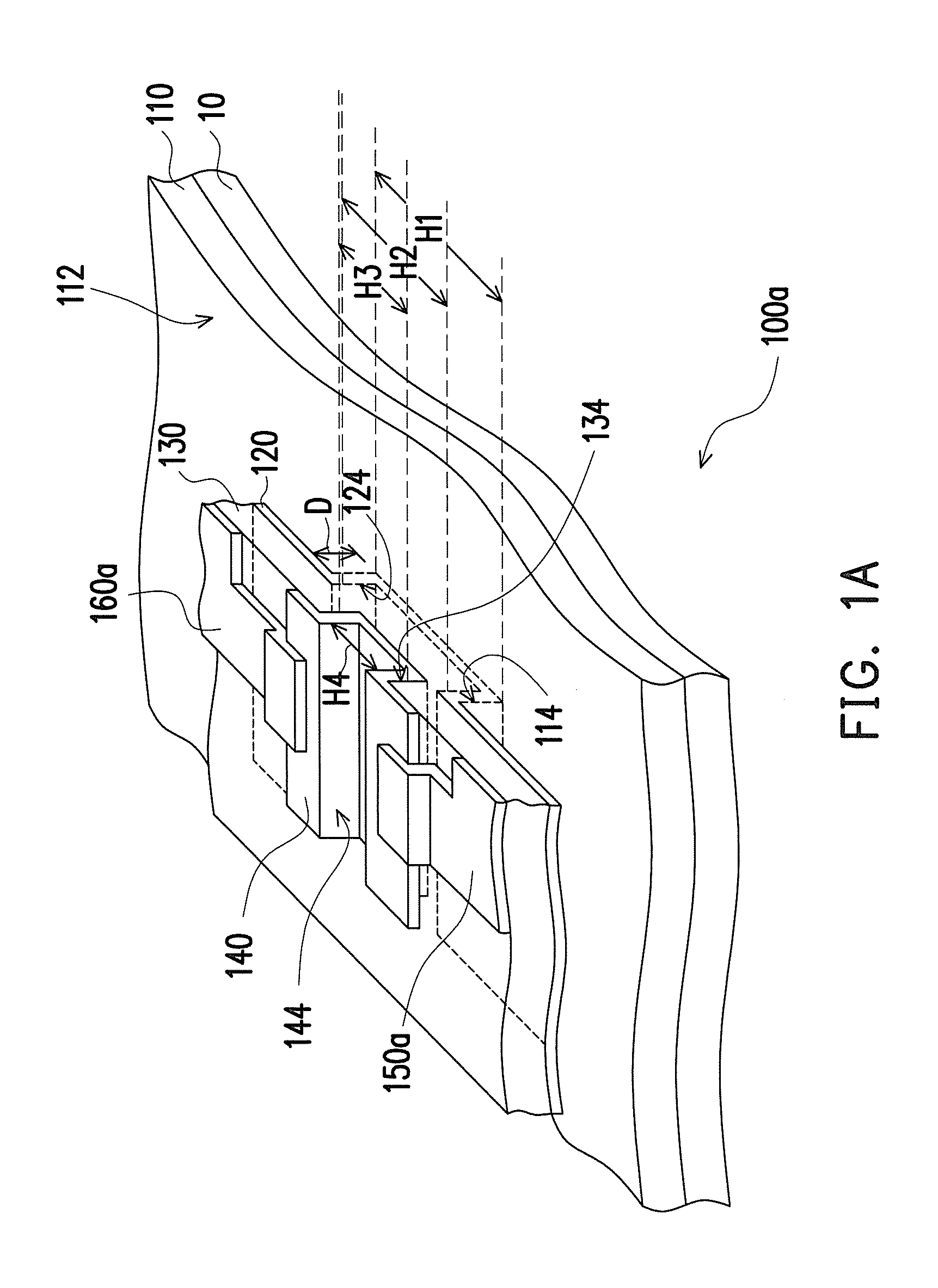
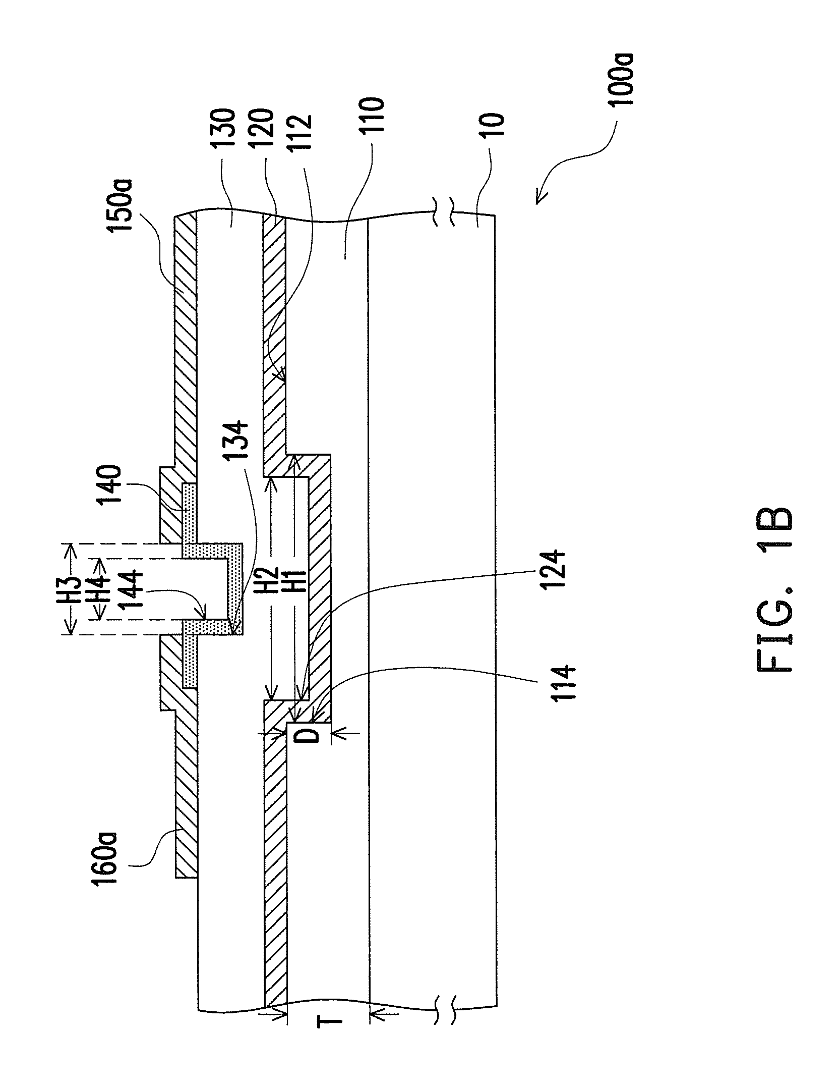
[0027]FIG. 1A is a schematic three-dimensional diagram of a semiconductor device according to an embodiment of the invention and FIG. 1B is a cross-sectional diagram of the semiconductor device of FIG. 1A. Referring to FIGS. 1A and 1B, a semiconductor device 100a of the embodiment is disposed on a base-plate 10, and the semiconductor device 100a includes a substrate 110, a metal layer 120, an insulating layer 130, a semiconductor layer 140, a drain 150a and a source 160a. The semiconductor device 100a herein is an active device, for example, a TFT.

[0028]In more details, the substrate 110 has a surface 112 and a first cavity 114 located at the surface 112. In the embodiment, a material of the substrate 110 is, for example, organic material or inorganic material, wherein the organic material is, for example, polyimide (PI) or polysiloxane (PSI), while the inorganic is, for example, silicon-oxide (SiOx) or silicon-nitride (SiNx). In addition, a depth D of the first cavity 114 is, for e...


PUM

PropertyMeasurementUnit
thicknessaaaaaaaaaa
opening diameteraaaaaaaaaa
conductiveaaaaaaaaaa

Abstract

A semiconductor device including a substrate, a metal layer, an insulating layer, a semiconductor layer, a drain and a source is provided. The substrate has a surface and a first cavity. The metal layer is disposed on the substrate and covers the surface and inner-wall of the first cavity to define a second cavity corresponding to the first cavity. The insulating layer covers the metal layer and inner-wall of the second cavity to define a third cavity corresponding to the second cavity. The semiconductor layer exposes out a portion of the insulating layer and covers the inner-wall of the third cavity to define a fourth cavity corresponding to the third cavity. The drain and source are disposed on the semiconductor layer and covers a portion of the semiconductor layer and a portion of the insulating layer, in which the drain and source expose out the fourth cavity.

Description

CROSS-REFERENCE TO RELATED APPLICATION[0001]This application claims the priority benefit of Taiwan application serial no. 101106741, filed on Mar. 1, 2012. The entirety of the above-mentioned patent application is hereby incorporated by reference herein and made a part of this specification.BACKGROUND OF THE INVENTION[0002]1. Field of the Invention[0003]The invention generally relates to a semiconductor device, and more particularly, to a semiconductor device in three-dimensional figure.[0004]2. Description of Related Art[0005]In recent years, thanks to progress of semiconductor process technology, the manufacturing of thin film transistor (TFT) gains easier and faster. TFT has quite broad applications, for example, in computer chip, mobile chip or thin film transistor liquid crystal display (TFT LCD). Taking the TFT LCD as an example, the TFT therein is used as charging or discharging switches to control the displaying of every pixel.[0006]Along with the higher and higher demands o...

Claims


Application Information

Patent Timeline
Patent Type & Authority Applications(United States)
IPC IPC(8): H01L29/786
CPCH01L29/41733H01L29/78603H01L29/786H01L27/1218H01L27/124H01L29/78696
Inventor LAN, WEI-CHOUSHINN, TED-HONGWANG, HENRYYEH, CHIA-CHUN
Owner E INK HLDG INC
Why Eureka
Try Eureka