Substrate processing apparatus and substrate processing method using same

a substrate processing and substrate technology, applied in the direction of electrical equipment, electrical discharge tubes, decorative arts, etc., can solve the problems of difficult to perform a stable substrate process, excessive amplitude (vpp) of bias rf power, etc., and achieve the effect of efficient plasma generation

Active Publication Date: 2010-09-30
TOKYO ELECTRON LTD
View PDF5 Cites 18 Cited by
  • Summary
  • Abstract
  • Description
  • Claims
  • Application Information

AI Technical Summary

Benefits of technology

[0010]In view of the above, the present invention provides a substrate processing apparatus and method which is capable of adjusting timings of output variation including ON / OFF of an excitation power applying device and output variation including ON / OFF of a bias power applying device and suppressing an amplitude (Vpp) of bias RF power from being increased, thereby preventing a problem such as abnormal discharge and the like from occurring.
[0011]Further, the present invention also provides a substrate processing apparatus and method capable of adjusting timings of output variation including ON / OFF of an excitation power applying device and output variation including ON / OFF of a DC voltage apply part for applying a bias DC voltage to a lower electrode, thereby suppressing heat from being generated due to the DC voltage and preventing the bias DC voltage applying part from being damaged due to load increase.

Problems solved by technology

However, in such a substrate processing method, if a balance is disturbed between an ON / OFF control of a RF power supply for plasma generation (hereinafter referred to as “excitation power applying device”) and an ON / OFF control of a RF power supply for bias (hereinafter referred to as “bias power applying device”), an amplitude (Vpp) of bias RF power may become excessively large, which may result in abnormal discharge and / or damage of an RF matching part of a matching unit, thereby making it difficult to perform a stable substrate process.

Method used


Image

  • Substrate processing apparatus and substrate processing method using same
  • Substrate processing apparatus and substrate processing method using same
  • Substrate processing apparatus and substrate processing method using same

Examples


first embodiment

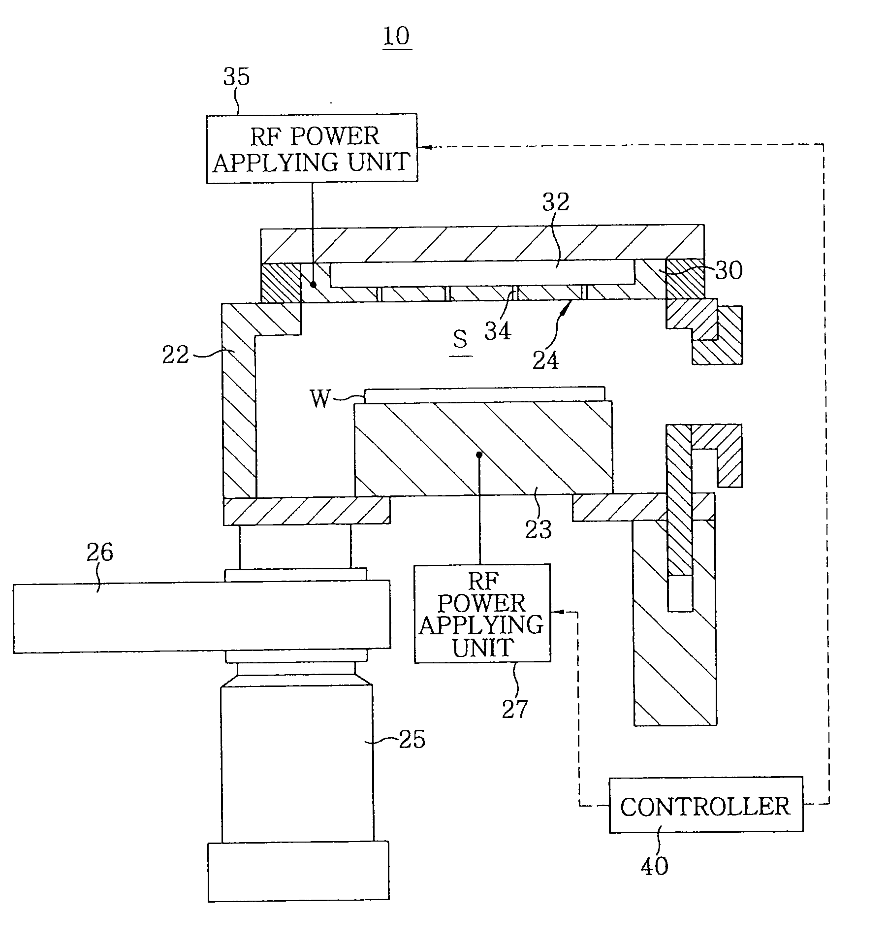
[0058]Hereinafter, the substrate processing method of the present invention will be described.

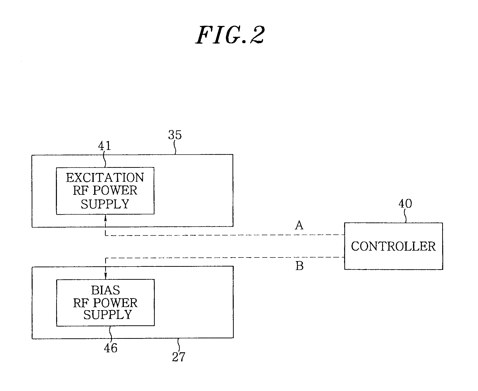
[0059]FIG. 3 is a timing diagram of the first embodiment of the substrate processing method of the present invention, showing timings at which the outputs of the RF power applying unit (hereinafter referred to as “RF1”) 35 and the RF power applying unit (hereinafter referred to as “RF2”) 27 are changed.

[0060]This embodiment represents a case where a pulse control, which allows outputs of both of RF1 and RF2 to be periodically changed, is performed and a pulse duration of RF1 is set to be smaller than that of RF2.

[0061]In FIG. 3, RF1 is ON / OFF-controlled with a predetermined period. When RF1 is in the ON state, an output with a predetermined waveform is applied to, e.g., the upper electrode 24. In FIG. 3, the control depicted in the lower side dashed box represents a control in accordance with this embodiment and the control depicted in the upper side dashed box represents a control for a co...

second embodiment

[0076]Next, the substrate processing method of the present invention will be described.

[0077]FIG. 6 is a timing diagram of a second embodiment of the substrate processing method of the present invention. This embodiment represents a case where both of RF1 and RF2 are pulse-controlled and a pulse duration of RF1 is set to be larger than that of RF2.

[0078]In FIG. 6, RF1 is ON / OFF-controlled with a predetermined period. When RF1 is in the ON state, an output with a predetermined waveform is applied from RF1 to, e.g., the upper electrode 24. In FIG. 6, the control depicted in the upper side dashed box represents a control for comparative example and the control depicted in the lower side dashed box represents a control in accordance with this embodiment.

[0079]In this example, the pulse duration of RF1 is set to be larger than that of RF2, and in the control for the comparative example depicted in the upper side dashed box, RF1 remains in the ON state while a state of RF2 becomes ON / OFF ...

third embodiment

[0084]Next, the substrate processing method of the present invention will be described.

[0085]FIG. 7 is a timing diagram of a third embodiment of the substrate processing method of the present invention. This embodiment represents a case where only RF1 is pulse-controlled while RF2 remains in the ON state.

[0086]In FIG. 7, RF1 is ON / OFF-controlled with predetermined equi-intervals. When RF1 is in the ON state, an output with a predetermined waveform is applied from RF1 to, e.g., the upper electrode 24. In FIG. 7, the control depicted in the upper side dashed box represents a control for comparative example and the control depicted in the lower side dashed box represents a control in accordance with this embodiment.

[0087]Since RF2 remains in the ON state while RF1 is ON / OFF-controlled with the predetermined equi-intervals, there occurs a case where RF2 is in the ON state with RF1 in the OFF state. In this case, Vpp (amplitude) of the RF power in RF2 becomes large, which results in abno...


PUM

PropertyMeasurementUnit
pulse frequencyaaaaaaaaaa
frequencyaaaaaaaaaa

Abstract

A substrate processing method uses a substrate processing apparatus including a chamber for accommodating a substrate, a lower electrode to mount the substrate, a first RF power applying unit for applying an RF power for plasma generation into the chamber, and a second RF power applying unit for applying an RF power for bias to the lower electrode. The RF power for plasma generation is controlled to be intermittently changed by changing an output of the first RF power applying unit at a predetermined timing. If no plasma state or an afterglow state exists in the chamber by a control of the first RF power applying unit, an output of the second RF power applying unit is controlled to be in an OFF state or decreased below an output of the second RF power applying unit when the output of the first RF power applying unit is a set output.

Description

CROSS-REFERENCE TO RELATED APPLICATIONS[0001]This application claims priority to Japanese Patent Application No. 2009-086035 filed on Mar. 31, 2009 and U.S. Provisional Application No. 61 / 242,650 filed on Sep. 15, 2009, the entire contents of which are incorporated herein by reference.FIELD OF THE INVENTION[0002]The present invention relates to a substrate processing apparatus and a substrate processing method using same, and, more particularly, to a substrate processing apparatus and method for subjecting a substrate to a predetermined process using a plasma generated when a process gas is excited.BACKGROUND OF THE INVENTION[0003]When wiring and the like are formed on a substrate such as a semiconductor wafer, the substrate is required to be subjected to a fine processing and a substrate processing method using a plasma has been widely employed therefor.[0004]The reactive ion etching (RIE) is widely employed in the field of semiconductor processing to process semiconductor devices,...

Claims


Application Information

Patent Timeline
Patent Type & Authority Applications(United States)
IPC IPC(8): C23F1/08C23F1/00
CPCH01J37/32091H01J37/02H01J37/32165H01J37/32146
Inventor OHSE, TAKESHIHIMORI, SHINJIABE, JUNYAMADA, NORIKAZU
Owner TOKYO ELECTRON LTD
Why Eureka
Try Eureka