Semiconductor integrated circuit

a technology of integrated circuits and semiconductors, applied in the direction of voltage/current interference elimination, oscillation generators, reliability increasing modifications, etc., can solve the problems that the fluctuation range of the crossover voltage may not meet the design specifications such as the usb specification, so as to suppress the fluctuation range of the crossover voltage

Inactive Publication Date: 2010-10-28
RENESAS ELECTRONICS CORP
View PDF3 Cites 15 Cited by
  • Summary
  • Abstract
  • Description
  • Claims
  • Application Information

AI Technical Summary

Benefits of technology

[0028]The circuit configuration as described above can suppress the fluctuation range of the crossover voltage.
[0029]According to the present invention, it is possible to provide a semiconductor integrated circuit capable of suppressing the fluctuation range of the crossover voltage.

Problems solved by technology

That is, if the power supply voltage VDD fluctuates for some reason, a fluctuation range of the crossover voltage may not meet the design specifications such as the USB specification.
This poses a problem that, if the power supply voltage VDD fluctuates for some reason, the fluctuation range of the crossover voltage may not meet the design specifications such as the USB specification.

Method used


Image

  • Semiconductor integrated circuit
  • Semiconductor integrated circuit
  • Semiconductor integrated circuit

Examples


first exemplary embodiment

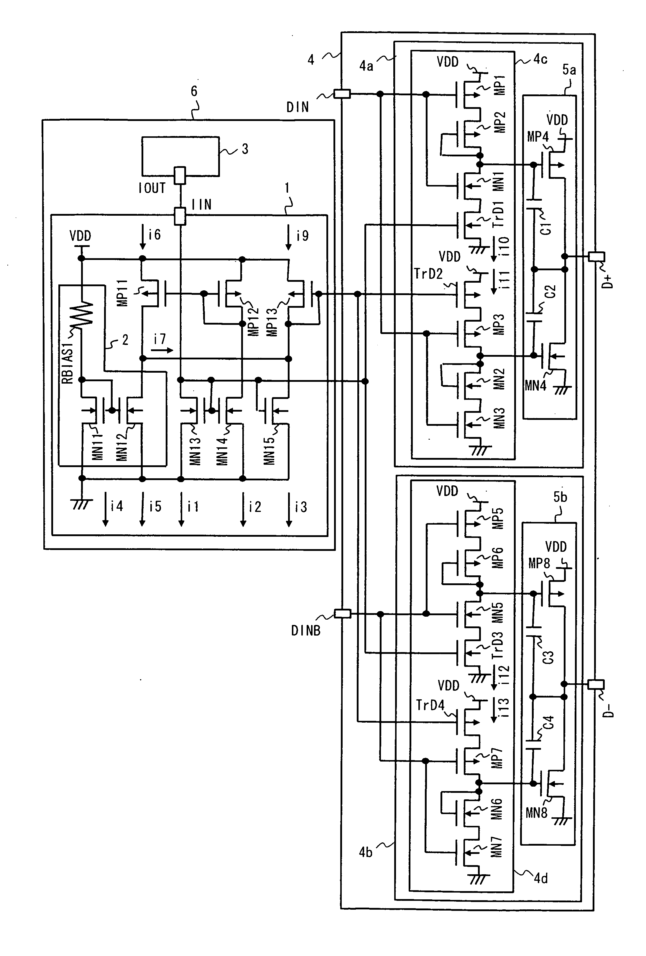
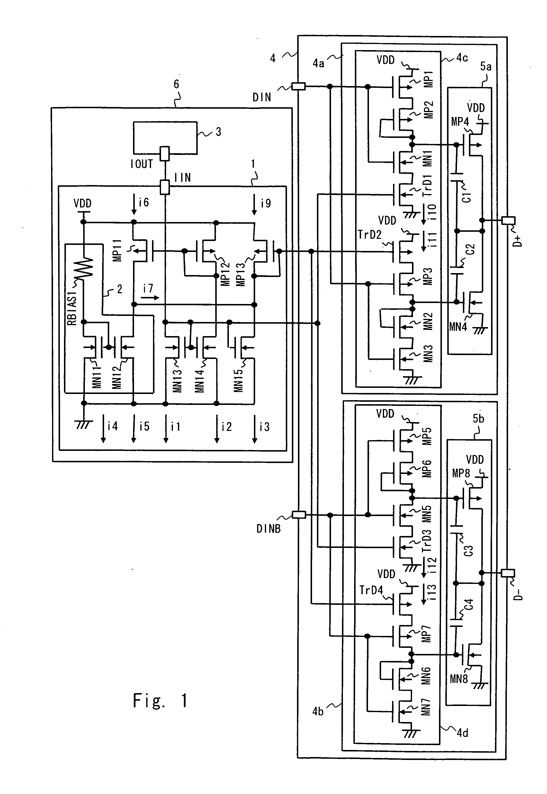
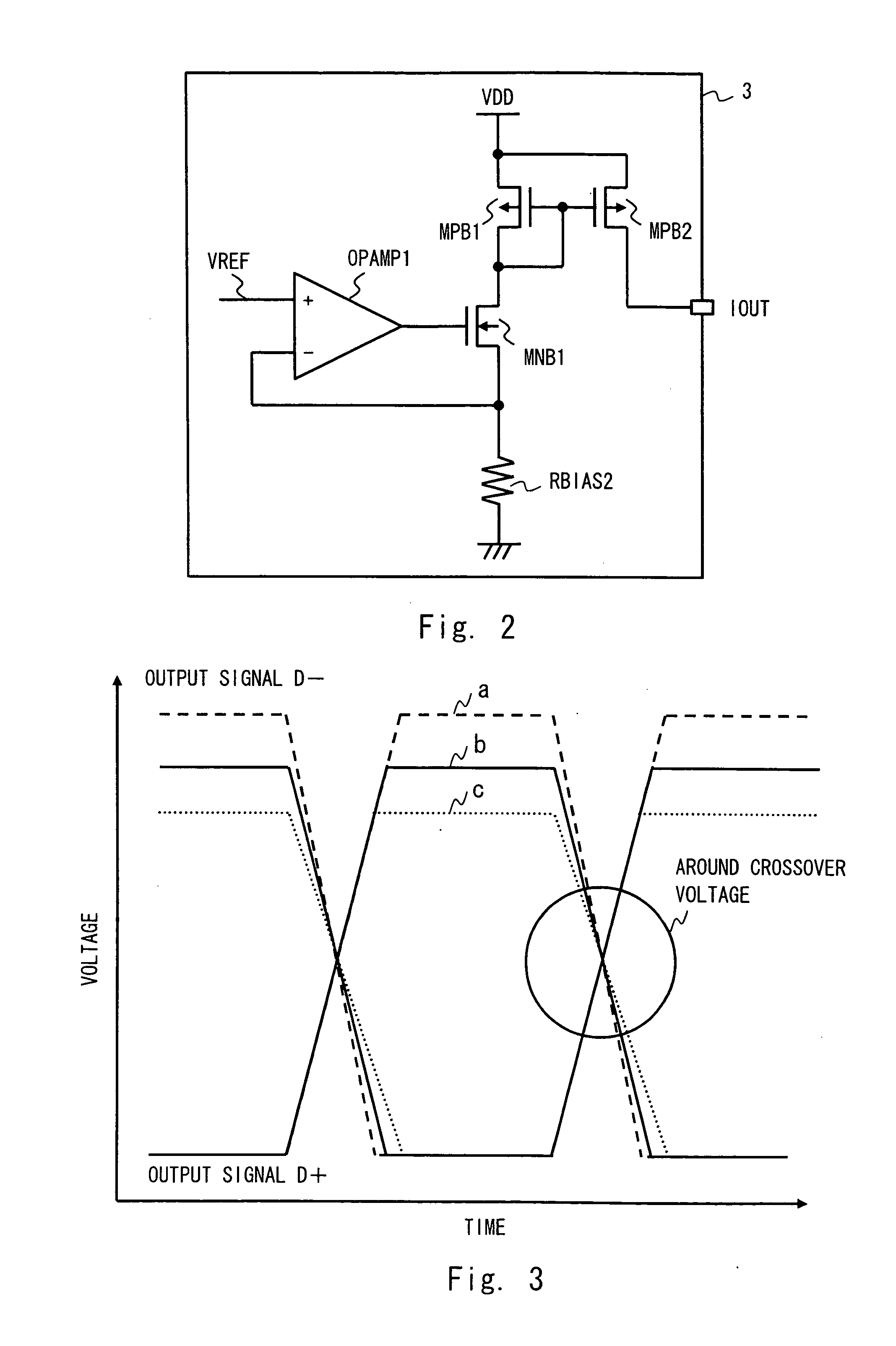
[0037]A semiconductor integrated circuit according to an exemplary embodiment of the present invention will be described with reference to the drawings. FIG. 1 is a diagram showing the semiconductor integrated circuit according to an exemplary embodiment of the present invention. The circuit shown in FIG. 1 is a differential drive circuit including an output circuit 5a (first output circuit), an output circuit 5b (second output circuit), a predriver 4c (first predriver circuit), a predriver 4d (second predriver circuit), and a control signal generation circuit 6. Each of the output circuits 5a and 5b has an integrator circuit configuration. The predrivers 4c and 4d drive the output circuits 5a and 5b, respectively. The control signal generation circuit 6 controls drive currents.

[0038]The circuit shown in FIG. 1 has a feature that a drive current for controlling “rise” (rising edge) of each of output signals D+ and D− is set as a constant current and a drive current for controlling “...


PUM


Abstract

Provided is a semiconductor integrated circuit including: a differential driver that is, disposed between a first power supply and a second power supply and drives differential input signals to generate differential output signals; and a control signal generation circuit that generates a first control signal for controlling a voltage level of each of the differential output signals. When each of a pair of output signals forming the differential output signals is changed from a voltage level corresponding to the first power supply to a voltage level corresponding to the second power supply, an amount of change in the voltage level of the corresponding output signal is controlled based on the first power supply.

Description

INCORPORATION BY REFERENCE[0001]This application is based upon and claims the benefit of priority from Japanese patent application No. 2009-108688, filed on Apr. 28, 2009, the disclosure of which is incorporated herein in its entirety by reference.BACKGROUND[0002]1. Field of the Invention[0003]The present invention relates to a semiconductor integrated circuit, and more particularly, to a driver circuit including a slew rate control circuit.[0004]2. Description of Related Art[0005]USB (Universal Serial Bus) interfaces are used with a wide range of peripheral devices. Examples of standard peripheral devices using USB interfaces include a mouse, a keyboard, a disk drive, a printer, and audio / video equipment.[0006]In order to transfer highly reliable information through a USB interface, it is important to improve the quality of the waveform of signals to be transmitted to and received from a transceiver. When communications are conducted at full speed and low speed, for example, even i...

Claims


Application Information

Patent Timeline
Patent Type & Authority Applications(United States)
IPC IPC(8): H03L5/00
CPCH03K19/00361
Inventor AZETSUJI, MOTOSHI
Owner RENESAS ELECTRONICS CORP
Why Eureka
Try Eureka