Clock generator to reduce long term jitter

Active Publication Date: 2010-09-30
SAMSUNG ELECTRONICS CO LTD +1
View PDF5 Cites 11 Cited by
  • Summary
  • Abstract
  • Description
  • Claims
  • Application Information

AI Technical Summary

Benefits of technology

[0007]A clock according to an exemplary embodiment of the inventive concept includes a controller, a digital PLL circuit, a charge pump PLL circuit, and a divider. The controller generates a division factor and a first internal clock signal in response to the low-frequency reference clock signal and a multiplication factor. The digital PLL circuit generates a second internal clock signal in response to the low-frequency reference clock signal, the division factor and the first internal clock signal. The charge pump PLL circuit generates a plurality of third internal clock signals by using the second internal clock signal. The divider generates the high-frequency clock signal in response to a phase selection signal, the division factor and the third internal clock signals.
[0008]The controller may include a counter, a first register block, a second register block, a first subtractor, a frequency lock detector, a third register block, a second subtractor, an adder, a fourth register block, and a digitally controlled oscillator. The counter counts the first internal clock signal. The first register block stores the output signal of the counter in response to the low-frequency reference clock signal. The second register block stores the output signal of the first register block in response to the low-frequency reference clock signal. The first subtractor calculates a difference between the output signals of the first and second register blocks. The frequency lock detector determines whether the frequency of the low-frequency reference clock signal is locked. The third register block generates and stores the division factor by using the output signal of the frequency lock detector and the multiplication factor according to the low-frequency reference clock signal. The second subtractor calculates a difference between the output signal of the first subtractor and the division factor. The adder performs an AND operation on the output signal of the second subtractor and a delayed signal to generate a 0th internal clock signal. The fourth register block stores the 0th internal clock signal in response to the low-frequency reference clock signal. The digitally controlled oscillator generates the first internal clock signal in response to the 0th internal clock signal.
[0009]The digital PLL circuit may include a frequency phase detector, a first coarse time-to-digital converter, a hierarchical time-to-digital converter, a first loop filter, a second loop filter, a third loop filter, a sigma delta converter, a digitally controlled oscillator, and an internal divider. The frequency phase detector compares the frequency and phase of the low-frequency reference clock signal to those of a divided signal and generates an up signal and a down signal. The first coarse time-to-digital converter generates a first converted signal by using the up signal and the down signal according to the first internal clock signal. The hierarchical time-to-digital converter generates a second converted signal by using the up signal and the down signal. The first loop filter filters part of a plurality

Problems solved by technology

If the pixel clock signal generated by the pixel clock generator does not have a regular phase, an image reproduced by using the pixel clock signal may not be properly displayed.
An irregular phase of the pixel clock signal may be caused by long term jitter.
For a charge pump PLL, which generates a high frequency signal by using a low frequency signal, long term jitter may be generated

Method used


Image

  • Clock generator to reduce long term jitter
  • Clock generator to reduce long term jitter
  • Clock generator to reduce long term jitter

Examples


Embodiment Construction

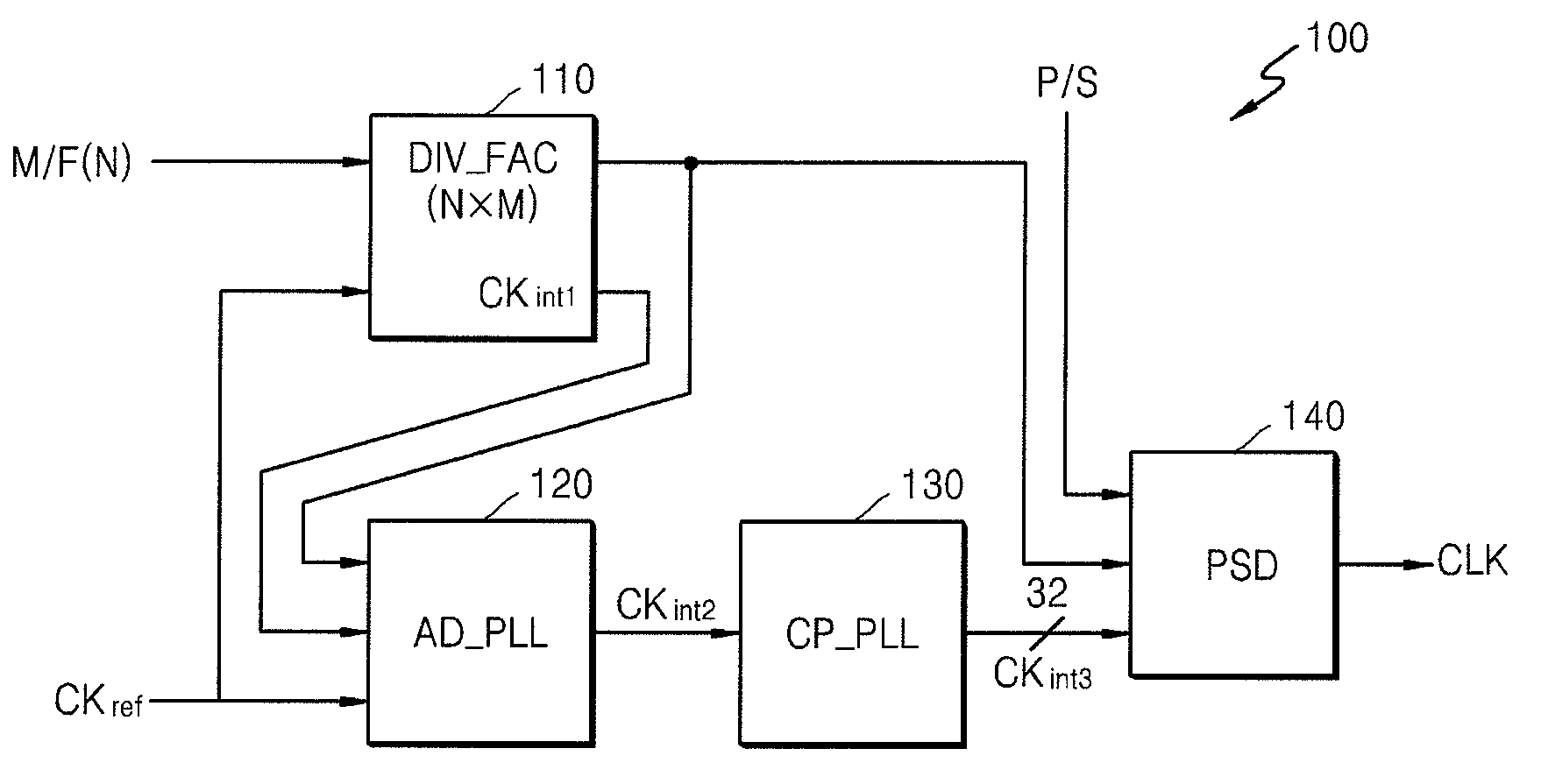
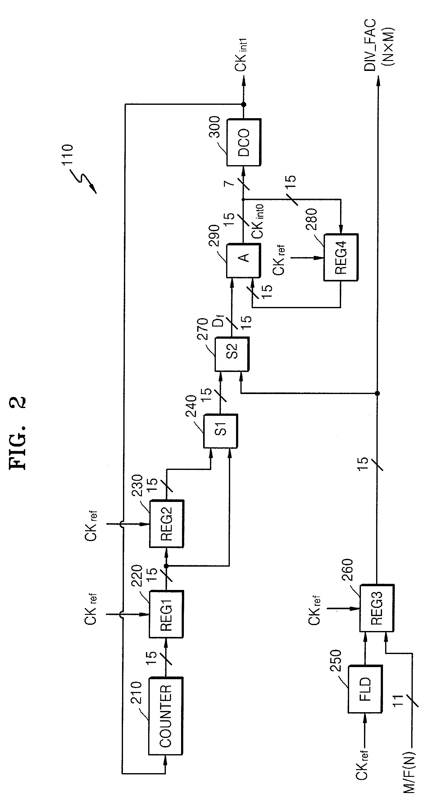
[0018]Hereinafter, the inventive concept will be described in detail by explaining exemplary embodiments thereof with reference to the attached drawings. Like reference numerals in the drawings denote like elements.

[0019]A clock generator according to at least one exemplary embodiment of the inventive concept converts an input low-frequency signal into a high-frequency signal having a frequency corresponding to an M×N multiple of the frequency of the low-frequency signal by using a digital PLL circuit, filters noise generated in the digital PLL circuit, and increases the frequency of the output signal of the digital PLL circuit by using a charge pump PLL circuit to minimize the generation of jitter and maximize the dynamic range of the output clock signal. The value N may be applied from an external device and the value M may be automatically determined by an internal controller of the clock generator. The clock generator may divide a signal generated by the charge pump PLL circuit ...


PUM


Abstract

A clock generator includes a controller, a digital phase locked loop (PLL) circuit, a charge pump phase locked loop (PLL) circuit and a divider. The controller generates a division factor and a first internal clock signal in response to a low-frequency reference clock signal and a multiplication factor. The digital PLL circuit generates a second internal clock signal in response to the reference clock signal, the division factor and the first internal clock signal. The charge pump PLL circuit generates a plurality of third internal clock signals by using the second internal clock signal. The divider generates a high-frequency clock signal in response to a phase selection signal, the division factor and the third internal clock signals.

Description

CROSS-REFERENCE TO RELATED APPLICATIONS[0001]This application claims priority to Korean Patent Application No. 10-2009-0026948, filed on Mar. 30, 2009, in the Korean Intellectual Property Office, the disclosure of which is incorporated by reference in its entirety herein.BACKGROUND[0002]1. Technical Field[0003]Embodiments of the inventive concept relate to a clock generator used in a display driver, and more particularly, to a clock generator to reduce long term jitter.[0004]2. Discussion of Related Art[0005]A digital signal converted from an analog video signal may be reproduced through corresponding pixels of an image to generate a viewable image corresponding to the analog video signal. A pixel clock signal may be used to temporally and spatially reproduce the digital signal converted from the analog video signal. The pixel clock signal may be synchronized with a horizontal synchronous signal and have a specific frequency and phase. The pixel clock signal may be generated by a pi...

Claims


Application Information

Patent Timeline
IPC IPC(8): H03L7/06
CPCH03L7/085H03L7/0991H03L2207/50H03L7/23H03L2207/06H03L7/1075H03L7/087H03L7/093
Inventor KIM, CHUL-WOOKIM, WOO-SEOKSONG, MIN-YOUNGPARK, JAE-JINKIM, JI-HYUNKWAK, YOUNG-HO
Owner SAMSUNG ELECTRONICS CO LTD
Why Eureka
Try Eureka