Liquid crystal display device

Active Publication Date: 2010-09-30
PANASONIC LIQUID CRYSTAL DISPLAY CO LTD +1
View PDF6 Cites 28 Cited by
  • Summary
  • Abstract
  • Description
  • Claims
  • Application Information

AI Technical Summary

Benefits of technology

[0023]According to the present invention, due to the above-mentioned constitution (3) where the black matrix is formed on the counter substrate and the support columns are arranged to fall within the black matrix forming region, there is no possibility that image quality is deteriorated due to the presence of the support columns.
[0024]According to the present invention, due to the above-mentioned constitution (4) where the gate signal lines are formed on the TFT substrate, the common electrode auxiliary lines are arranged along the gate signal lines, and the pedestals are formed of the metal film which is arranged in the inside of the opening portions formed in the common electrode auxiliary line in an island shape, the metal film which constitutes the pedestals easily reflects light emitted from a backlight and hence, there exists a large possibility that image quality is influenced by the light. However, in the present invention, the light which may be incident on the pedestal is blocked by the gate signal line and hence, the deterioration of image quality can be suppressed. Fur

Problems solved by technology

Accordingly, it becomes difficult to maintain the distance betwee

Method used


Image

  • Liquid crystal display device
  • Liquid crystal display device
  • Liquid crystal display device

Examples


embodiment 1

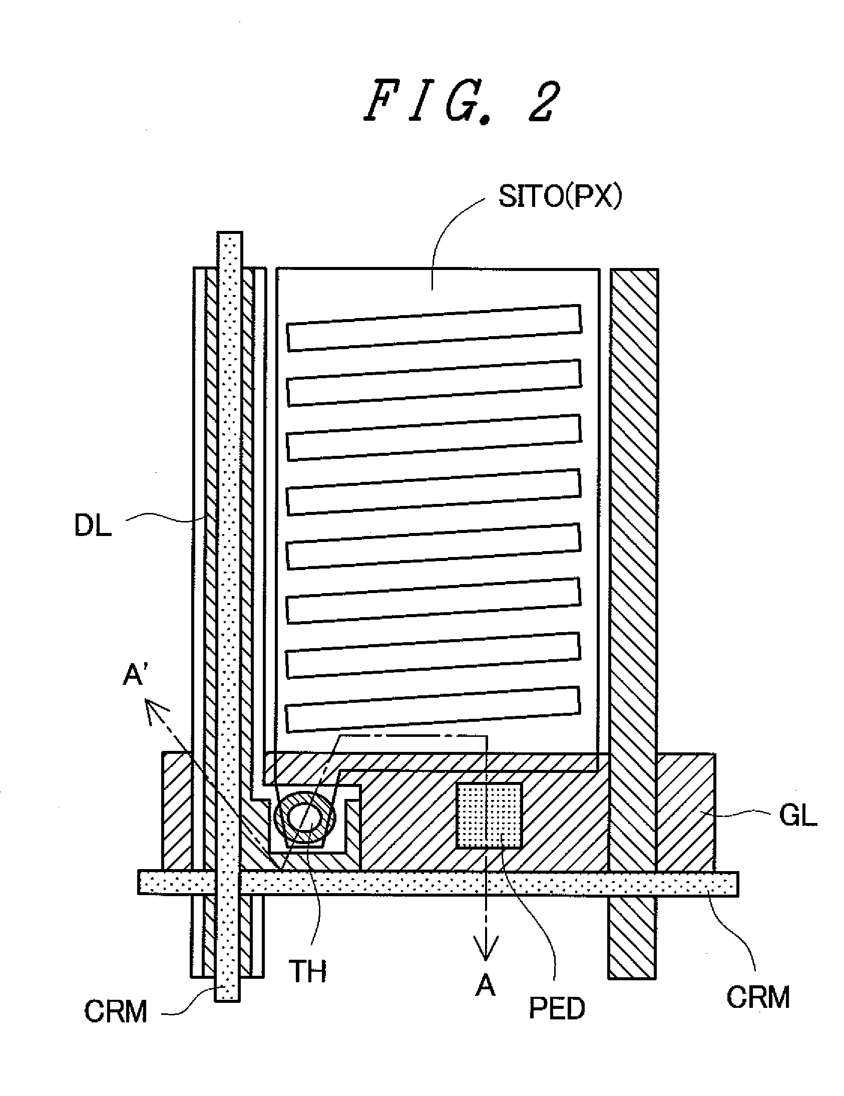
[0057]Next, the liquid crystal display device according to the embodiment 1 of the present invention is explained in conjunction with FIG. 2 to FIG. 4. FIG. 2 is a plan view showing a portion of the TFT substrate, and FIG. 3 is a cross-sectional view of the liquid crystal display device taken along a line A-A′ in FIG. 2.

[0058]As shown in FIG. 3, the support columns SOC are arranged on a surface of a leveling layer OC which covers the black matrix BM arranged on a surface of the counter substrate SUB2 not shown in the drawing in a state where the support columns SOC face the TFT substrate SUB1 in an opposed manner. On a surface of the leveling layer OC, an alignment film (not shown in the drawing) for controlling the alignment of liquid crystal LC is formed.

[0059]To explain a method of manufacturing the support columns SOC, a photosensitive resin is applied to an upper surface of the leveling layer OC, and is dried by heating. Then, the photosensitive resin is exposed using a mask pa...

embodiment 2

[0068]A liquid crystal display device according to the embodiment 2 of the present invention is explained in conjunction with FIG. 5 to FIG. 7.

[0069]FIG. 5 is a plan view of the liquid crystal display device showing a portion of a TFT substrate in the same manner as FIG. 2. FIG. 6 is a cross-sectional view taken along a line A-A′ in FIG. 5. FIG. 7 is a view showing a state of a common electrode CT on the periphery of a gate signal line GL in the same manner as FIG. 4.

[0070]The technical feature of the second embodiment lies in that, as shown in FIG. 5 and FIG. 7, a width of a common electrode auxiliary line CRM which is arranged along a gate signal line GL formed on a TFT substrate SUB1 is increased such that the width becomes substantially equal to a width of the gate signal line GL. A pedestal PED is arranged inside an opening portion formed in the common electrode auxiliary line CRM in an island shape. Further, an opening portion is also formed in a portion of the common electrod...


PUM


Abstract

A liquid crystal display device can properly maintain a distance between a TFT substrate and a counter substrate even when an organic film which constitutes color filters or the like is formed on a TFT substrate and pedestals are formed on the organic film. In a liquid crystal display device which includes a TFT substrate, a counter substrate and liquid crystal sandwiched between the TFT substrate and the counter substrate, support columns SOC which project toward a TFT substrate are formed on the counter substrate, thin film transistors, an insulation film PAS1 which covers the thin film transistors, organic films (color filter CF(G), CF(R)) which are arranged on the insulation film, and a transparent electrode CITO which constitutes a common electrode and is arranged on portions of organic films are formed on the TFT substrate, at least portions of the transparent electrode include a metal film which constitutes a common electrode auxiliary line CRM respectively, and portions of the metal film which are arranged on the transparent electrode form pedestals PED corresponding to the support columns SOC.

Description

[0001]The present application claims priority from Japanese application JP2009-079233 filed on Mar. 27, 2009, the content of which is hereby incorporated by reference into this application.BACKGROUND OF THE INVENTION[0002]1. Field of the Invention[0003]The present invention relates to a liquid crystal display device and a manufacturing method thereof, and more particularly to a liquid crystal display device in which a predetermined distance is held between a TFT substrate and a counter substrate by a support column system and a manufacturing method thereof.[0004]2. Background Art[0005]In a liquid crystal display device, liquid crystal is filled in a space formed between a TFT substrate on which pixel electrodes and thin film transistors (TFT) are formed and a counter substrate on which color filters and the like are formed, and images are formed by controlling molecules of the liquid crystal by an electric field. The distance (cell gap) between the TFT substrate and the counter subs...

Claims


Application Information

Patent Timeline
IPC IPC(8): G02F1/1343G02F1/1333G02F1/1335
CPCG02F1/133512G02F1/13394G02F2201/40G02F1/136286G02F2001/136222G02F1/134363G02F1/136222
Inventor ONO, KIKUO
Owner PANASONIC LIQUID CRYSTAL DISPLAY CO LTD
Why Eureka
Try Eureka