Adjusting access of non-volatile semiconductor memory based on access time

a non-volatile semiconductor and access time technology, applied in the field can solve the problem of reducing the overall performance (throughput) of non-volatile semiconductor memory

Active Publication Date: 2010-09-30
WESTERN DIGITAL TECH INC
View PDF100 Cites 167 Cited by
  • Summary
  • Abstract
  • Description
  • Claims
  • Application Information

AI Technical Summary

Problems solved by technology

This may be undesirable since excessive polling for the status command register consumes power in battery operated host devices.
However, while transferring the next command to the first memory device, the second memory device may also be ready to receive a next command but must wait for t

Method used


Image

  • Adjusting access of non-volatile semiconductor memory based on access time
  • Adjusting access of non-volatile semiconductor memory based on access time
  • Adjusting access of non-volatile semiconductor memory based on access time

Examples


Embodiment Construction

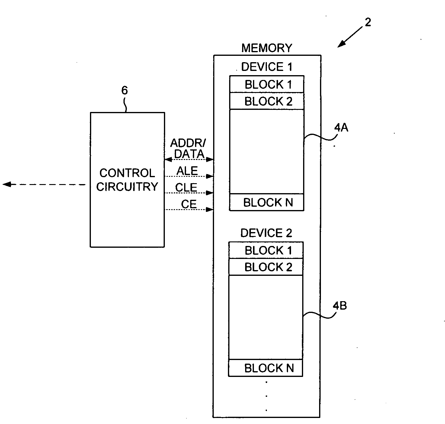
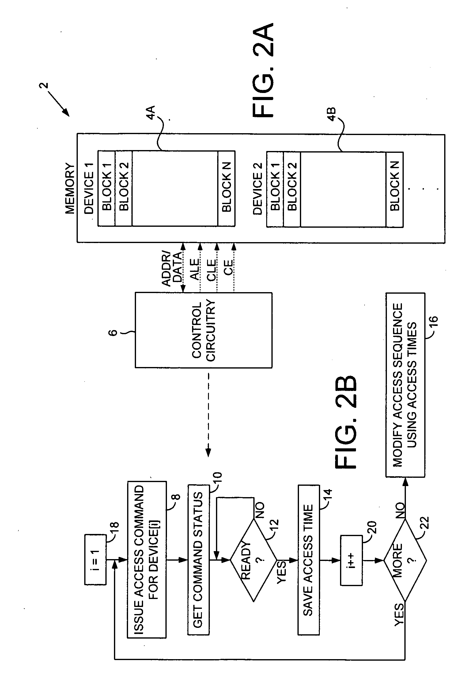
[0015]FIG. 2A shows a non-volatile semiconductor memory 2 according to an embodiment of the present invention comprising a first memory device 4A and control circuitry 6 operable to execute the flow diagram shown in FIG. 2B. An access command is issued to the first memory device (step 8). A command status is requested from the first memory device after a status delay (step 10). When the command status indicates the first memory device has completed the command (step 12), a first access time of the memory device is measured (step 14). An access sequence of the first memory device is then modified in response to the access time (step 16).

[0016]The memory device 4A in the embodiment of FIG. 2A may comprise any suitable device, such as a NAND flash memory. A typical NAND flash memory is accessed by transmitting a corresponding address and transmitting / receiving data over an address / data bus (ADDR / DATA), and asserting appropriate control lines (e.g., address latch enable (ALE), command l...


PUM


Abstract

A non-volatile semiconductor memory is disclosed comprising a first memory device and control circuitry operable to issue an access command to the first memory device. A command status is requested from the first memory device after a status delay. When the command status indicates the first memory device has completed the command, a first access time of the memory device is measured. An access sequence of the first memory device is then modified in response to the access time.

Description

BACKGROUNDDescription of the Related Art[0001]A non-volatile semiconductor memory may be employed as mass storage for a computer system (e.g., desktop, laptop, portable, etc.) or a consumer device (e.g., music player, cell phone, camera, etc.) or other suitable application. The non-volatile semiconductor memory may comprise one or more memory devices (such as a flash memory) and control circuitry for accessing each memory device. Each memory device is coupled to an address bus and a data bus, as well as a number of interface control lines. When issuing a write command or an erase command to a memory device, the control circuitry configures the address bus and control lines, and then transfers command data (and user data for a write operation) over the data bus. After receiving the command, the memory device executes the command internally over an “access time”. To determine when the memory device is finished executing the command, the control circuitry typically polls the memory dev...

Claims


Application Information

Patent Timeline
IPC IPC(8): G06F12/00G06F3/00
CPCG11C7/22G11C16/32G06F2212/7201G06F12/0246G11C2216/30
Inventor SYU, MEI-MAN L.
Owner WESTERN DIGITAL TECH INC
Why Eureka
Try Eureka