Semiconductor device and method of manufacturing the same

a semiconductor and semiconductor technology, applied in the field of semiconductor devices, can solve problems such as weakening of bonding force, and achieve the effect of preventing a reduction of bonding for

Inactive Publication Date: 2010-10-07
DENSO CORP
View PDF7 Cites 44 Cited by
  • Summary
  • Abstract
  • Description
  • Claims
  • Application Information

AI Technical Summary

Benefits of technology

[0007]In view of the above, it is an object of the present invention to provide a semiconductor device including two substrates bonded together and having a structure for preventing a reduction in a bonding force at an interface between the substrates. It is another object of the present invention to provide a method of manufacturing the semiconductor device.

Problems solved by technology

Further, after the stacked wafer is diced into individual chips, each chip may be subjected to external force that can weaken the bonding force between the sealing metal layer and each portion.

Method used


Image

  • Semiconductor device and method of manufacturing the same
  • Semiconductor device and method of manufacturing the same
  • Semiconductor device and method of manufacturing the same

Examples


first embodiment

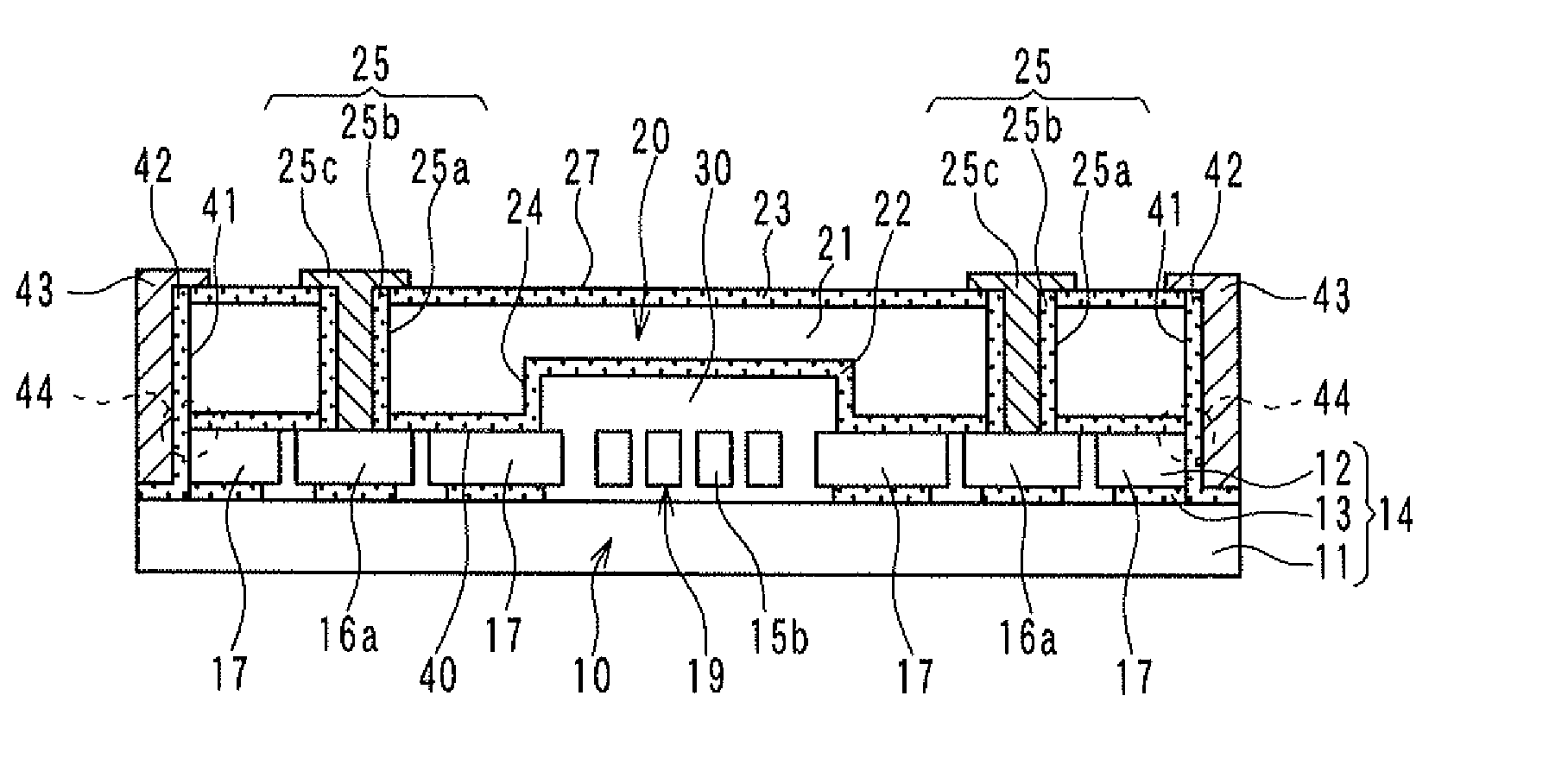
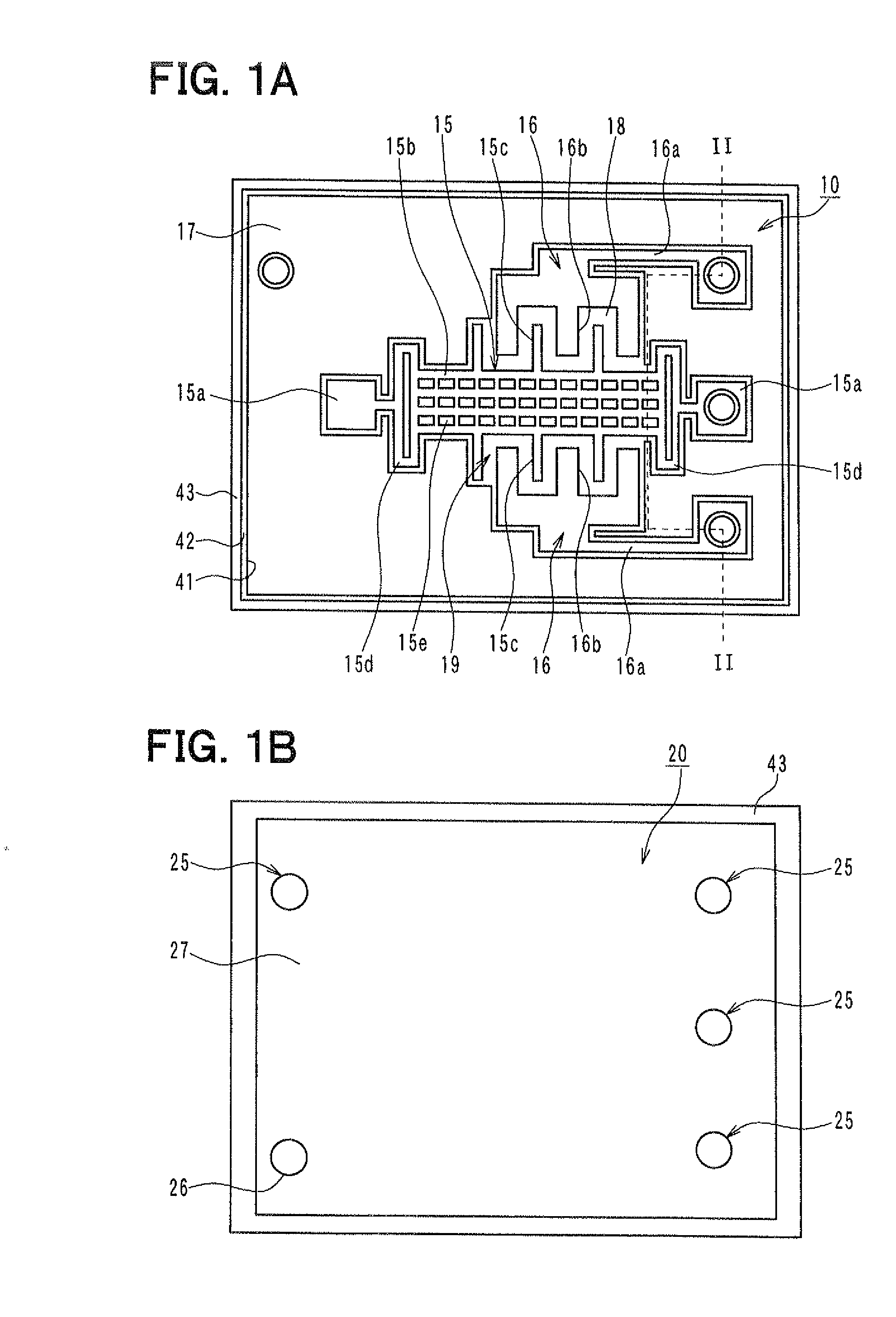
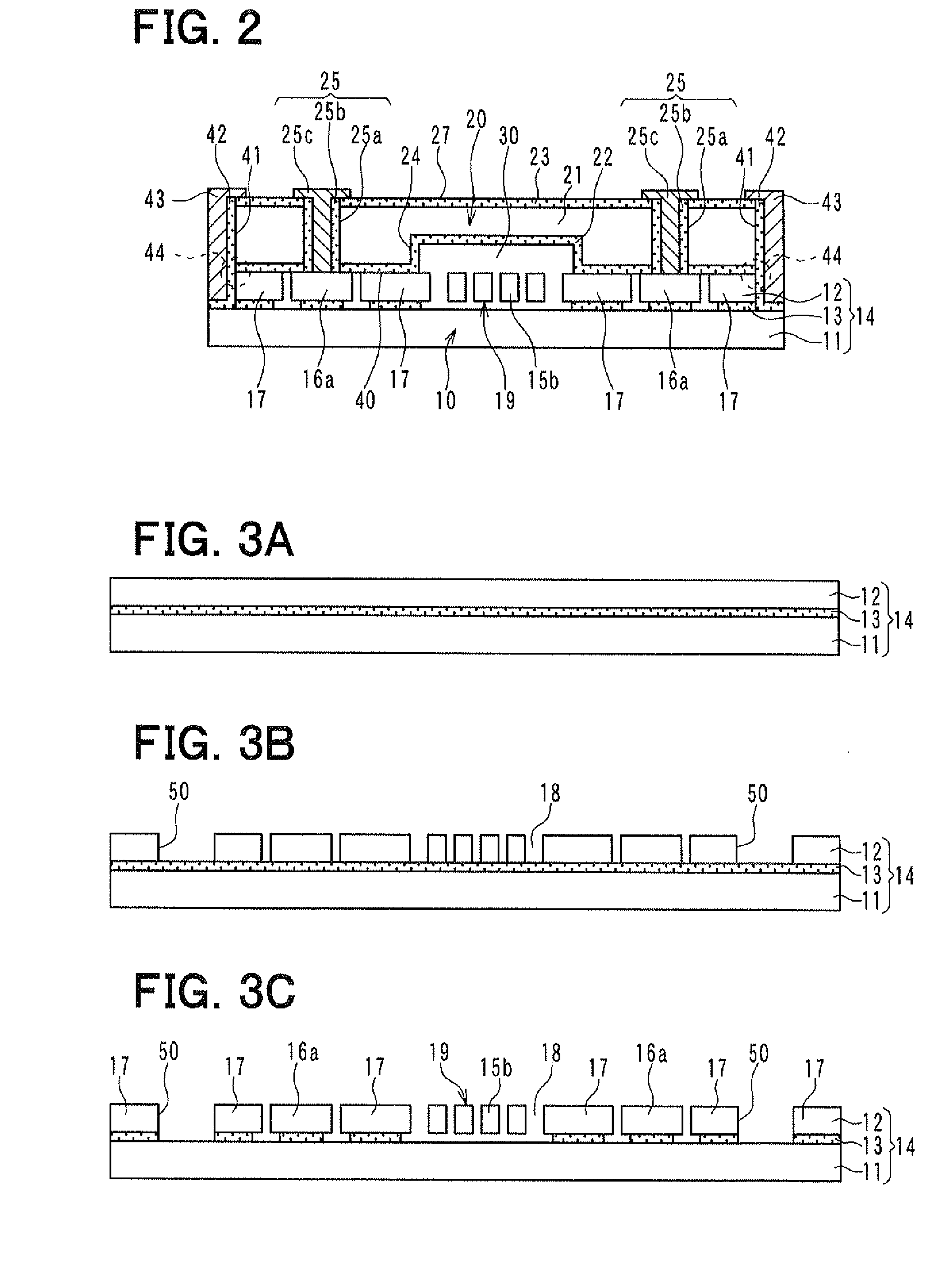
[0038]A semiconductor device according to a first embodiment of the present invention is described below with reference to FIGS. 1A and 1B, and FIG. 2. For example, the semiconductor device can be a dynamic quantity sensor having a movable portion such as an acceleration sensor for detecting an acceleration of a vehicle.

[0039]Referring to FIG. 2, the semiconductor device includes a sensor section 10 and a cap section 20 that are stacked on top of each other. FIG. 1A is a plan view of the sensor section 10. FIG. 1B is a plan view of the cap section 20. FIG. 2 is a cross-sectional view of the semiconductor device taken along the line II-II in FIG. 1A.

[0040]Firstly, the sensor section 10 is described. The sensor section 10 is configured to detect a physical quantity such as an acceleration. As shown in FIG. 2, the sensor section 10 is based on a silicon-on-insulator (SOI) substrate 14 including a supporting substrate 11, a semiconductor layer 12, and a sacrificial layer 13. The sacrifi...

second embodiment

[0105]A semiconductor device according to a second embodiment of the present invention is described below with reference to FIGS. 7A, 7B, and 8. A difference between the first and second embodiments is as follows. In the first embodiment, the stacked wafer 52 is diced into individual semiconductor devices by dicing the insulation layer 42 and the metal sealing layer 43. In contrast, in the second embodiment, the stacked wafer 52 is diced into individual semiconductor devices by dicing a portion outside the insulation layer 42 and the metal sealing layer 43.

[0106]FIG. 7A is a plan view of a cap section 20 of the semiconductor device according to the second embodiment, and FIG. 7B, corresponding to FIG. 2, is a cross-sectional view of the semiconductor device according to the second embodiment.

[0107]As shown in FIG. 7B, the recess 41, the insulation layer 42, and the sealing metal layer 43 are located closer to the center of the semiconductor device than the side surface of the semico...

third embodiment

[0111]A semiconductor device according to a third embodiment of the present invention is described below with reference to FIG. 9. FIG. 9, corresponding to FIG. 2, is a cross-sectional view of the semiconductor device according to the third embodiment. A difference between the third embodiment and the first embodiment is as follows.

[0112]According to the third embodiment, as shown in FIG. 9, the recess 41 penetrates at least the interface 40 between sensor section 10 and the cap section 20. In other words, the recess 41 is recessed in a side surface 45 of the semiconductor device so that at least the interface 40 between the sensor section 10 and the cap section 20 can be located in the recess 41. The recess 41 can fully surround the side surface 45 of the semiconductor device. Alternatively, the recess 41 can partially surround the side surface 45 of the semiconductor device.

[0113]The sealing metal layer 43 is located in the recess 41 to fill the sealing metal layer 43 so that the ...


PUM


Abstract

A semiconductor device includes a first semiconductor substrate, a second semiconductor substrate, and a sealing member. The first semiconductor substrate has a surface and includes a sensing portion on the surface side. The sensing portion has a movable portion. The first semiconductor substrate and the second semiconductor substrate are bonded together to form a stacked substrate. The stacked substrate defines a hermetically sealed space for accommodating the sensing portion between the first and second semiconductor substrates. The stacked substrate further defines a recess extending between the first semiconductor substrate and the second semiconductor substrate to penetrate an interface between the first semiconductor substrate and the second semiconductor substrate. The sealing member is located in the recess.

Description

CROSS REFERENCE TO RELATED APPLICATION[0001]This application is based on and incorporates herein by reference Japanese Patent Application No. 2009-91793 filed on Apr. 6, 2009 and No. 2010-53399 filed on Mar. 10, 2010.FIELD OF THE INVENTION[0002]The present invention relates to a semiconductor device having at least two substrates bonded together and also relates to a method of manufacturing the semiconductor device.BACKGROUND OF THE INVENTION[0003]Conventionally, there has been proposed a wafer level package structure. For example, JP-2005-251898A discloses a structure including a first substrate having a first sealing metal layer disposed around an element and a second substrate having a second sealing metal layer that is located facing the first sealing metal layer. In the structure, the first and second metal layers are joined together through a third conductor so that the element in the first substrate can be hermetically sealed between the first and second substrates.[0004]The ...

Claims


Application Information

Patent Timeline
Patent Type & Authority Applications(United States)
IPC IPC(8): H01L29/84H01L21/50
CPCB81B7/0041B81C2203/019H01L23/3121H01L2924/0002H01L2924/00
Inventor TANAKA, MASAYAFUJII, TETSUOYOKURA, HISANORI
Owner DENSO CORP
Why Eureka
Try Eureka