Power level indicator

Active Publication Date: 2010-10-07
TEXAS INSTR INC
View PDF4 Cites 29 Cited by
  • Summary
  • Abstract
  • Description
  • Claims
  • Application Information

AI Technical Summary

Benefits of technology

[0004]It is an object of the invention to provide an electronic device with an improved control

Problems solved by technology

If the power consumption of SYSTEM 5 exceeds the maximum available power, this can cause a sudden drop of

Method used


Image

  • Power level indicator
  • Power level indicator
  • Power level indicator

Examples


Example

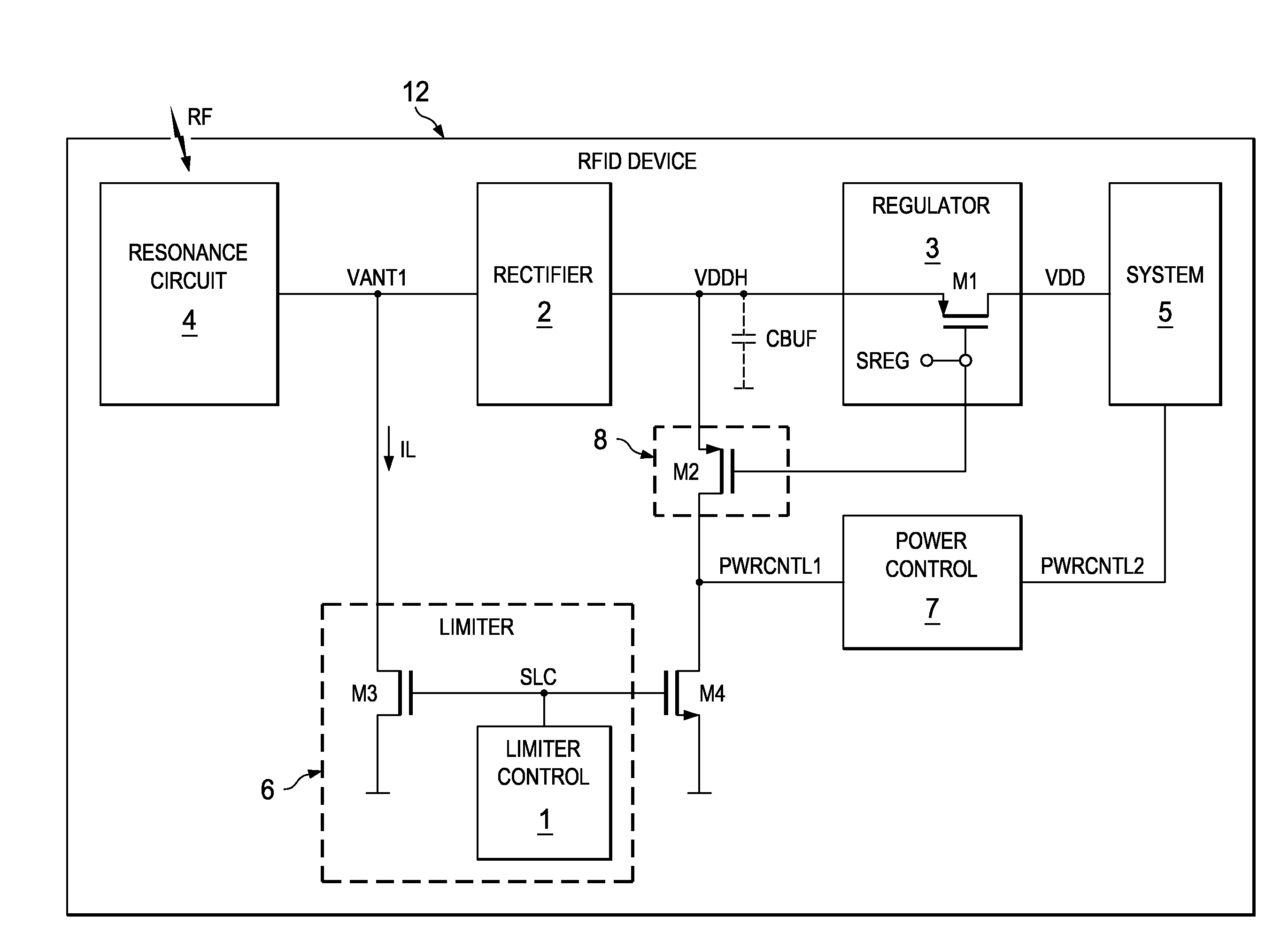
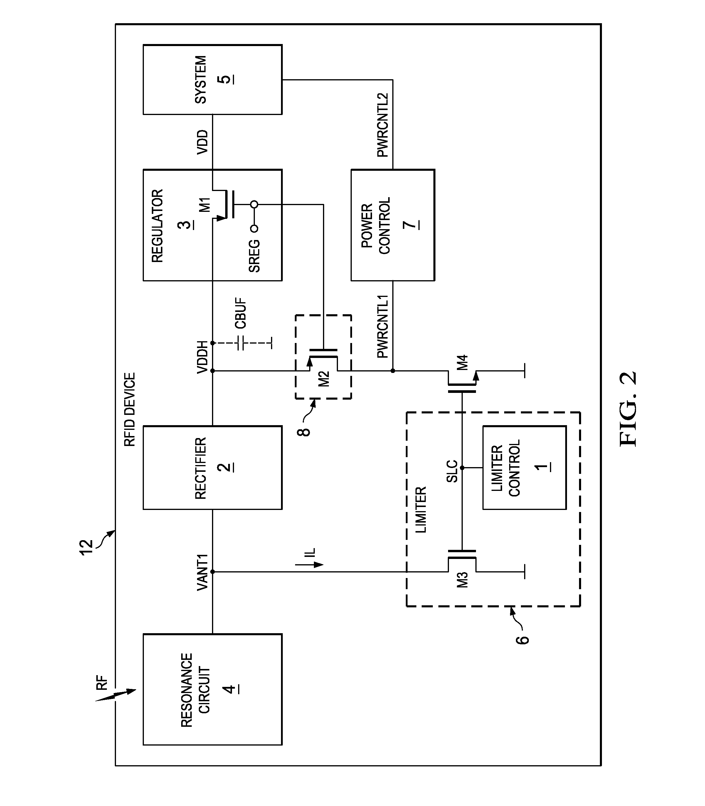
[0014]FIG. 2 shows a simplified circuit (and block) diagram of an electronic device 12 (e.g. a partially integrated electronic device as an RF transponder IC) according to an embodiment of the invention. The basic structure and components of the electronic device 12 are substantially similar to the RFID device 10 shown in FIG. 1. There is a resonant circuit (LR, CR), which may include a resonance inductor LR and a resonance capacitor CR shown in FIG. 1. The resonance circuit 4 is excited with an external RF signal, i.e. it serves as antenna. The incoming RF signal or electronic field induces a voltage at node VANT1. A limiter 6 is coupled to node VANT1. The limiter 6 includes a limiter control stage 1, which provides a limiter control signal SLC to transistor M3. Transistor M3 is coupled with a channel to VANT1 for presenting a variable load to node VANT1. If the voltage at node VANT1 exceeds a maximum limit, limiter control stage 1 controls M3 through limiter control signal SLC to ...


PUM


Abstract

An electronic device is provided that is adapted to generate a supply voltage at an input node from a radio frequency (RF) signal. The electronic device includes a limiter coupled to the input node for limiting a supply voltage level at the input node that is generated by the received RF signal. The limiter is configured to draw a limiter current from the input node so as to limit the supply voltage level to a maximum and a magnitude of the limiter current is used for controlling a power consumption of the electronic device.

Description

CROSS-REFERENCE TO RELATED APPLICATIONS[0001]This patent application claims priority from German Patent Application No. 10 2009 013 962.1, filed Mar. 20, 2009, the entirety which is incorporated herein by reference.FIELD OF THE INVENTION[0002]The present invention relates to a method and an electronic device with a mechanism for indicating a power level of an available amount of power.BACKGROUND OF THE INVENTION[0003]There is a ubiquitous need to improve power management of mobile electronic devices, as for example RFID transponders. A simplified circuit and block diagram of a conventional RFID device is shown in FIG. 1. The RFID device can be supplied through a received RF signal (electromagnetic waves, electromagnetic field). Therefore, the RFID device 10 includes a resonance circuit 4 with a resonant inductor LR (may serve as antenna) and resonant capacitor CR. The resonant circuit is excited through an external RF signal to oscillate with an oscillation frequency. Due to this os...

Claims


Application Information

Patent Timeline
IPC IPC(8): G05F3/02
CPCH02J17/00H02J50/20H02J50/12H02J50/80
Inventor NEHRIG, OLIVERPESCHKE, CARLO
Owner TEXAS INSTR INC
Why Eureka
Try Eureka