Display Device
Active Publication Date: 2010-11-04
SEMICON ENERGY LAB CO LTD
14 Cites 73 Cited by
AI-Extracted Technical Summary
Problems solved by technology
However, the display device equipped with a personal computer (PC) and the like significantly differs from the paper media such as newspapers and magazines in that the convenience such as portability is poor.
In that case, bending of the...
View moreBenefits of technology
[0018]In accordance with one embodiment of the present invention, a sturdy display device with less breaking of a driver circuit can be provided...
View moreAbstract
The display device includes: a flexible display panel including a display portion in which scanning lines and signal lines cross each other; a supporting portion for supporting an end portion of the flexible display panel; a signal line driver circuit for outputting a signal to the signal line, which is provided for the supporting portion; and a scanning line driver circuit for outputting a signal to the scanning line, which is provided for a flexible surface of the display panel in a direction which is perpendicular or substantially perpendicular to the supporting portion.
Application Domain
Technology Topic
Image
Examples
- Experimental program(5)
Example
Embodiment 1
[0039]In Embodiment 1, an example of a display device will be described with reference to drawings.
[0040]The display device described in Embodiment 1 includes the following: a flexible display panel including a display portion in which scanning lines and signal lines cross each other; a supporting portion for supporting an end portion of the flexible display panel; a signal line driver circuit for outputting a signal to the signal line, which is provided for the supporting portion; and a scanning line driver circuit for outputting a signal to the scanning line, which is provided for a flexible surface of the display panel in a direction which is perpendicular or substantially perpendicular to the supporting portion.
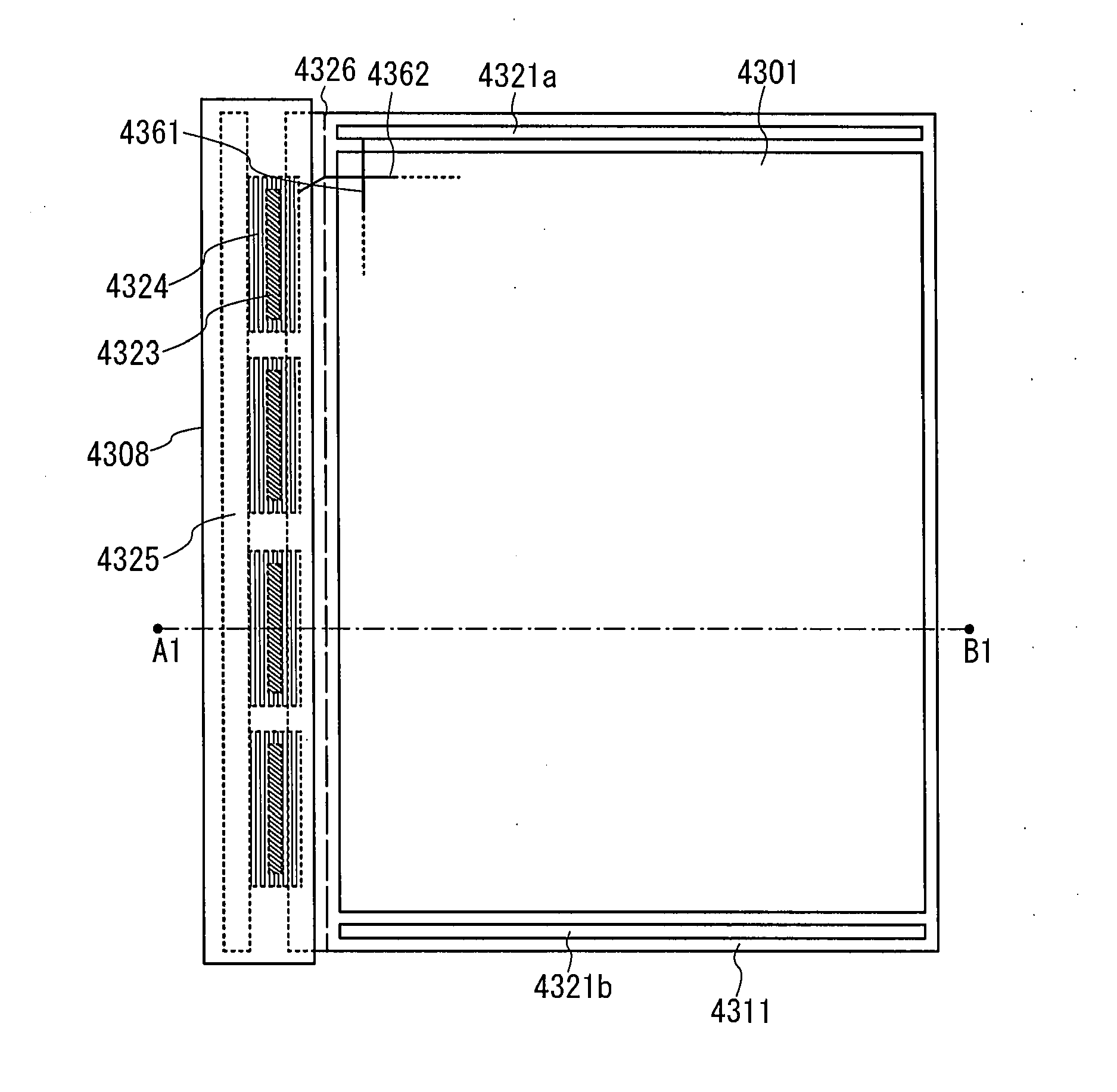
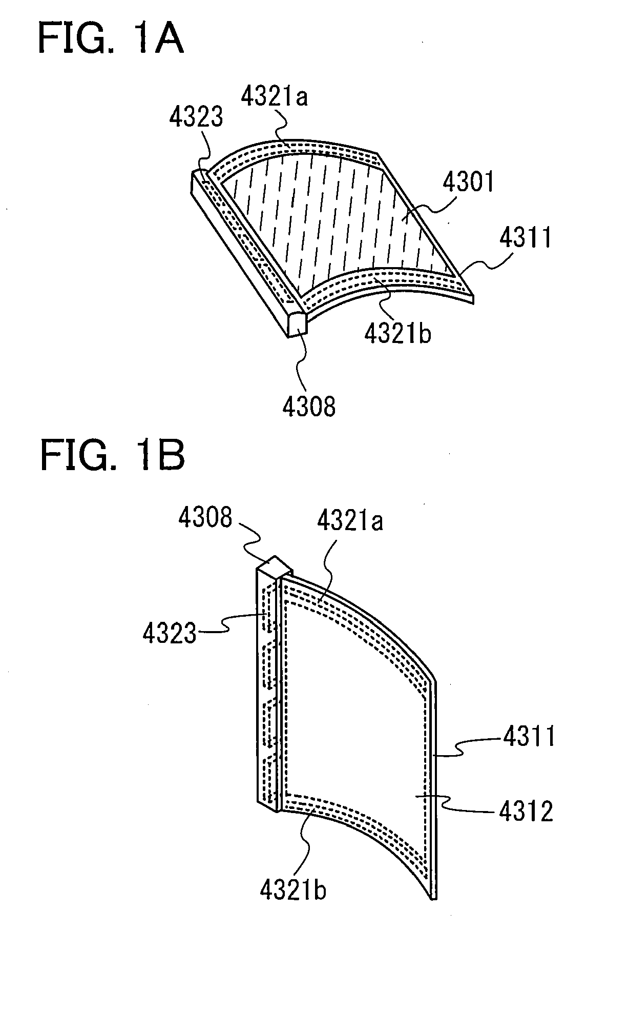
[0041]FIG. 1 illustrates the case where a supporting portion 4308 is provided at an end portion of a display panel 4311. A specific structure of the display device will be described using FIGS. 1A and 1B below. FIG. 1 illustrates the display device which is horizontally disposed, and FIG. 1B illustrates the display device which is vertically disposed.
[0042]The display device illustrated in FIGS. 1A and 1B includes the display panel 4311 including a display portion 4301, the supporting portion 4308 provided at an end portion of the display panel 4311, scanning line driver circuits 4321a and 4321b for controlling display on the display portion 4301, and a signal line driver circuit 4323 for controlling display on the display portion 4301.
[0043]The scanning line driver circuits 4321a and 4321b are provided for the display panel 4311 and the signal line driver circuit 4323 is provided inside the supporting portion 4308.
[0044]The display panel 4311 may be flexible. In that case, a pixel circuit included in the display portion 4301 and the scanning line driver circuits 4321a and 4321b may be provided over a flexible substrate such as a plastic substrate.
[0045]It is preferable that the supporting portion 4308 be less flexible (more rigid) than at least the display panel 4311. For example, a housing forming the supporting portion 4308 can be formed using plastic, metal, or the like which is thicker than the display panel 4311. In that case, the display device can be bent (warped) at a portion other than the supporting portion 4308.
[0046]There is no particular limitation on where to arrange the supporting portion 4308. For example, the supporting portion 4308 can be provided along an end portion of the display panel 4311. For example, as shown in FIGS. 1A and 1B, in the case where the display panel 4311 has a rectangular shape, the supporting portion 4308 can be provided along a predetermined side of the display panel 4311 (so that the side is fixed). Note that the “rectangular shape” here includes a shape in which a corner of the rectangular is rounded.
[0047]The signal line driver circuit 4323 is provided inside the supporting portion 4308. For example, the supporting portion 4308 is formed using a columnar housing with a hollow or a cylindrical housing with a hollow, and the signal line driver circuit 4323 can be provided in the hollow. When the signal line driver circuit 4323 is provided inside the supporting portion 4308, damage to the signal line driver circuit 4323 due to bending of the display panel 4311 can be prevented.
[0048]Further, as shown in FIGS. 1A and 1B, the scanning line driver circuits 4321a and 4321b are preferably provided at both end portions of the display panel 4311 in a direction parallel or substantially parallel to the supporting portion 4308. As a result, leading of a wiring can be reduced and the structure can be simplified in comparison with the case where the scanning line driver circuit and the signal line driver circuit are provided at one portion (e.g., the supporting portion 4308).
[0049]Further, the scanning line driver circuits 4321a and 4321b and the pixel circuit included in the display portion 4301 may be formed over a flexible substrate through the same process, so that the scanning line driver circuits 4321a and 4321b can be bent and cost reduction can be achieved.
[0050]The pixel circuit included in the display portion 4301 and the scanning line driver circuits 4321a and 4321b each can be formed using a thin film transistor or the like. On the other hand, a high-speed operation circuit such as the signal line driver circuit 4323 can be formed using an integrated circuit (IC) formed using a semiconductor substrate such as a silicon substrate or an SOI substrate, and the IC can be provided inside the supporting portion 4308.
[0051]When the IC including the high-speed operation circuit such as a signal line driver circuit is provided inside the supporting portion and the scanning line driver circuit and the pixel circuit included in the display portion are formed using elements such as thin film transistors over a flexible substrate as described above, the display panel can be bent easily, occurrence of breaking of the IC due to the bending of the display panel can be suppressed, and cost reduction can be achieved in comparison with the case where the signal line driver circuit and the scanning line driver circuit are provided using an IC. In addition, when the scanning line driver circuit is provided on the display panel at the end portion of the display panel in a direction perpendicular or substantially perpendicular to the supporting portion, leading of a wiring can be suppressed and the structure can be simplified.
[0052]Although the case where the scanning line driver circuit is provided at both end portions of the display panel 4311 is illustrated in FIGS. 1A and 1B, the scanning line driver circuit (either one of the scanning line driver circuit 4321a and the scanning line driver circuit 4321b) may be provided at one end portion.
[0053]Embodiment 1 can be implemented in appropriate combination with any structure described in the other embodiments.
Embodiment Mode 2
Example
[0054]In Embodiment 2, a specific structure of the above-described display device illustrated in FIGS. 1A and 1B will be described using drawings. The structures described in Embodiment 2 are in common with that described in Embodiment 1 in many points, and thus, in the description below, description of the common points will be omitted and different points will be described in detail.
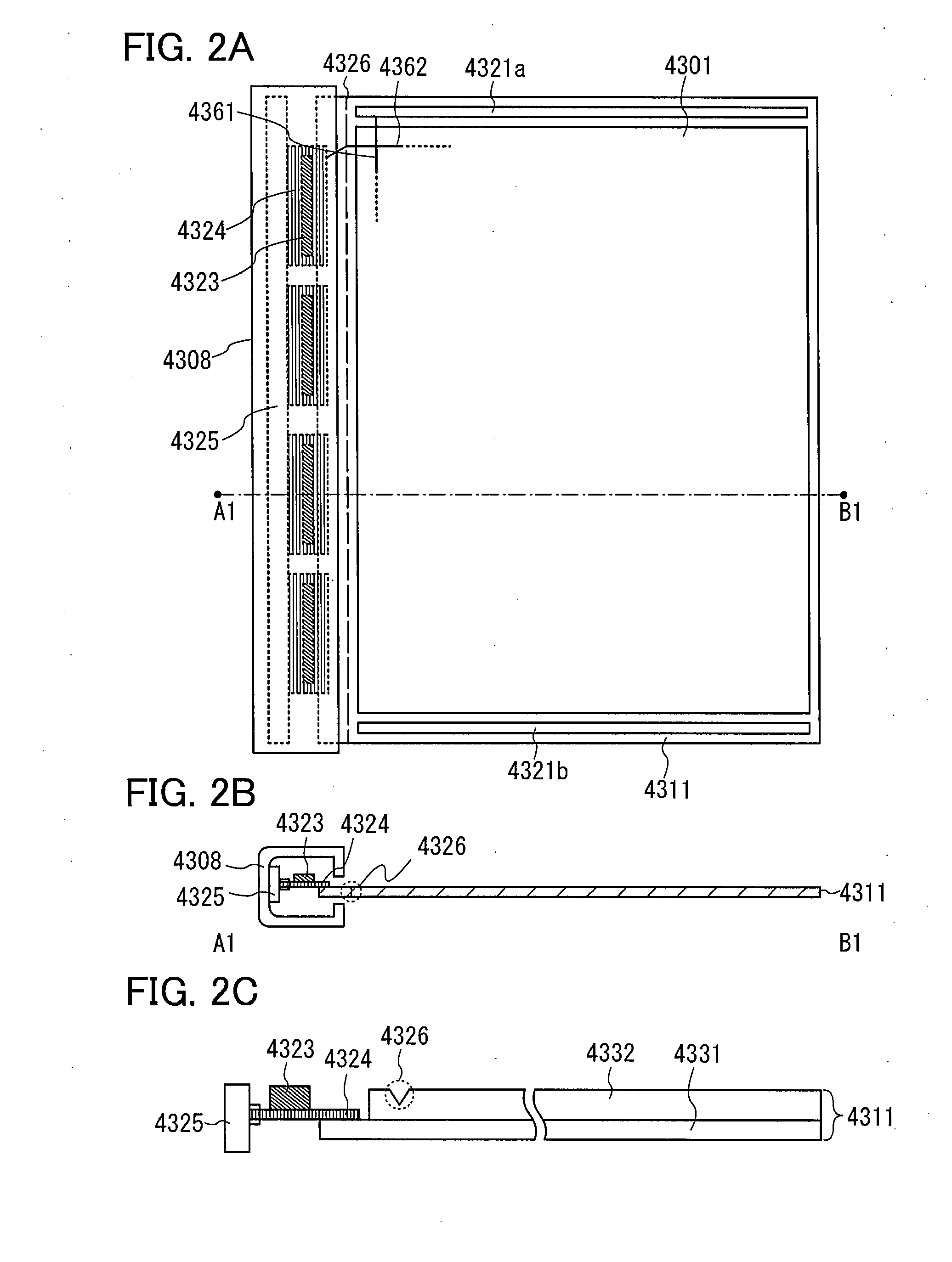
[0055]First, an example of the specific structure of the display device is described using FIGS. 2A to 2C. FIG. 2A is a plane view of the display device, FIG. 2B is a cross-sectional view along line A1-B1 of FIG. 2A, and FIG. 2C is a detailed schematic view of the cross section.
[0056]As for the display device shown in FIGS. 2A to 2C, the supporting portion 4308 is formed using a housing with a hollow, and the signal line driver circuit 4323 is provided inside the housing. In this embodiment, the signal line driver circuit 4323 is formed using an IC, and the IC is provided inside the supporting portion 4308. The IC can be formed using an SOI substrate, a semiconductor substrate such as a silicon substrate, or the like. Any circuit (e.g., a CPU, a memory) other than the signal line driver circuit can be provided for the IC as well.
[0057]Further, FIGS. 2A to 2C illustrate the case where the IC provided inside the supporting portion 4308 is mounted on a flexible printed circuit (FPC) by a tape automated bonding (TAB) method. More specifically, the signal line driver circuit 4323 for controlling the display portion 4301 is provided on an FPC 4324, and the FPC 4324 is electrically connected to a printed board 4325.
[0058]As shown in FIGS. 2A to 2C, the printed board 4325 can be provided to be in contact with the supporting portion 4308.
[0059]In the case where the signal line driver circuit 4323 is provided on the FPC 4324, it is preferable to provide a stress concentration region 4326 for the display panel 4311. The stress concentration region 4326 provided for the display panel makes it possible to reduce the stress which is applied to the FPC 4324 at the time when the display panel 4311 is bent and to suppress the occurrence of breaking of the signal line driver circuit 4323 provided on the FPC 4324.
[0060]The stress concentration region means a region where a stress formed by deformation of a material due to cutting or the like, change of the strength against bending and/or extension due to attachment of a material or the like, or the like is concentrated. Specifically, the stress concentration region 4326 can be formed by providing a cut portion (depression or groove) at a portion at which the display panel 4311 is bent.
[0061]For example, the display panel 4311 can be formed using an element substrate 4331 and a sealing substrate 4332, and one or both of the element substrate 4331 and the sealing substrate 4332 can be provided with a cut portion. FIGS. 2A to 2C illustrate the case where the cut portion is provided in the sealing substrate 4332 to form the stress concentration region 4326. In addition, in the structure described here, the scanning line driver circuits 4321a and 4321b and a pixel circuit which drives the display portion 4301 can be formed on the element substrate 4331, and these circuits can be electrically connected to the FPC 4324.
[0062]In the display portion 4301, pixels are arranged (disposed) in matrix, and scanning lines 4361 and signal lines 4362 are arranged so as to dissect at right angles. As for the arrangement of the pixels, the pixels may be arranged either linearly in a longitudinal direction and in a lateral direction or zigzag. Therefore, in the case of stripe arrangement or the case where dots for three colors are arranged in delta, the scanning lines 4361 and the signal lines 4362 are arranged depending on the pixel arrangement.
[0063]The stress concentration region 4326 may be provided along a direction in which the display panel 4311 is bent. For example, in FIG. 2A, the cut portion may be provided from an upper end to a bottom end of the display panel 4311 along a direction which is parallel to or substantially parallel to the supporting portion 4308, so that the direction in which the display panel 4311 is bent can be controlled (the display panel 4311 can be bent in a direction perpendicular to or substantially perpendicular to the supporting portion 4308 as selected) and the occurrence of breaking of the signal line driver circuit 4323 provided on the FPC 4324 can be suppressed.
[0064]The stress concentration region 4326 can be provided inside or outside the supporting portion 4308. For example, the stress concentration region 4326 is preferably provided outside the supporting portion 4308 (e.g., between the supporting portion 4308 and the display portion 4301) in the case where the supporting portion 4308 is provided so as to be close to the display panel 4311.
[0065]Next, a structure of the display device, which is different from that in FIGS. 2A to 2C is described using FIGS. 3A to 3C. FIG. 3A is a plane view of the display device, FIG. 3B is a cross-sectional view along line A2-B2 of FIG. 3A, and FIG. 3C is a detailed schematic view of the cross section.
[0066]FIGS. 3A to 3C illustrate the case where an IC where the signal line driver circuit 4323 is formed is mounted on the display panel 4311 by a chip on glass (GOG) method. More specifically, the signal line driver circuit 4323 for controlling the display portion 4301 is provided on the element substrate 4331 included in the display panel 4311, and the signal line driver circuit 4323 is electrically connected to the printed board 4325 through the FPC 4324.
[0067]As shown in FIGS. 3A to 3C, in the case where the signal line driver circuit is provided on the display panel, similarly to the case of FIGS. 2A to 2C, the stress concentration region 4326 is preferably provided for the display panel 4311. In this case, the stress concentration region 4326 is provided in a region which is different from (is provided so as to avoid) the region in which the signal line driver circuit 4323 is provided. For example, when the stress concentration region 4326 is provided on the sealing substrate 4332 side, the stress which is applied to the signal line driver circuit 4323 at the time when the display panel 4311 is bent can be reduced and the occurrence of breaking of the signal line driver circuit 4323 can be suppressed.
[0068]Next, a structure of the display device, which is different from those in FIGS. 2A to 2C and FIGS. 3A to 3C is described using FIGS. 4A to 4C. FIG. 4A is a plane view of the display device, FIG. 4B is a cross-sectional view along line A3-B3 of FIG. 4A, and FIG. 4C is a detailed schematic view of the cross section.
[0069]FIGS. 4A to 4C illustrate the case where an IC in which a circuit such as a signal line driver circuit is formed is provided on a printed board, and the printed board and a display panel are connected with an FPC. More specifically, the signal line driver circuit 4323 for controlling the display portion 4301 is provided on the printed board 4327, and the display panel 4311 and the signal line driver circuit 4323 are electrically connected to each other through the FPC 4324.
[0070]In FIGS. 4A to 4C, the display panel 4311 can be bent with the FPC 4324, and therefore a stress concentration region is not necessarily provided for the display panel 4311.
[0071]Next, examples of the supporting portion 4308 and a configuration of a circuit which can be provided for the supporting portion 4308 are described using FIG. 5.
[0072]FIG. 5 illustrates the case where a display control portion 200 including a signal line driver circuit is incorporated in the supporting portion 4308. Such a circuit can be formed using an IC formed using an SOI substrate, a semiconductor substrate such as a silicon substrate, or the like.
[0073]The display control portion 200 can include a CPU 201, a memory portion 203, a power feeding portion 205, a power supply circuit 207, an image signal generation circuit 215, the signal line driver circuit 4323, an operation portion 219, and the like. Those components can be connected to each other through an interface or the like. The display control portion 200 is electrically connected to the display panel 4311. Although the operation portion 219 is provided in the supporting portion 4308 in this case, the operation portion 219 can be provided on the display panel 4311.
[0074]The CPU 201 controls the operation of the whole display device.
[0075]Data to be displayed on the display portion 4301 is input to a data input portion 211 from an external device. Note that the data input portion 211 may include an antenna 216 for transmitting/receiving data to/from an external device. In that case, the data input portion 211 has a function of transferring data received by the antenna 216 or data stored in a memory medium (an external memory 213) to an internal memory 209.
[0076]The memory portion 203 can include the internal memory 209, the data input portion 211, and the external memory 213. Data to be displayed on the display portion 4301, a program for operating the display device, or the like can be recorded in the internal memory 209, the data input portion 211, and the external memory 213.
[0077]The internal memory 209 includes a memory portion for storing a program for processing a signal output to the image signal generation circuit 215 and/or the power supply circuit 207 on the basis of a signal from the power feeding portion 205, the operation portion 219, or the like, data transferred from the data input portion 211, or the like. As examples of the internal memory 209, a DRAM (dynamic random access memory), an SRAM (static random access memory), a mask ROM (read only memory), a PROM (programmable read only memory), and the like are given.
[0078]As an example of the external memory 213, a memory medium such as an IC card or a memory card is given.
[0079]The power feeding portion 205 includes a secondary battery, a capacitor, and the like. A reduction in size of the power feeding portion 205 is possible when, for example, a lithium battery, preferably, a lithium polymer battery utilizing a gel electrolyte, a lithium ion battery, or the like is used as the secondary battery. Needless to say, any battery can be used as long as it can be charged, and a battery that can be charged and discharged, such as a nickel-metal hydride battery, a nickel-cadmium battery, an organic radical battery, a lead storage battery, an air secondary battery, a nickel-zinc battery, or a silver-zinc battery may be used. As the capacitor, an electric double layer capacitor, a lithium ion capacitor, another capacitor with high capacitance, or the like can be used. The capacitor is preferably used because it is less likely to be deteriorated even if the number of charging and discharging is increased and is excellent in rapid charging. The shape of the power feeding portion 205 may be sheet-like, cylinder-like, prism-like, plate-like, coin-like, or the like, which can be selected as appropriate.
[0080]Further, the power feeding portion 205 can have a structure in which electric power is wirelessly supplied. In that case, an antenna may be provided for the power feeding portion 205.
[0081]The power supply circuit 207 is a circuit for controlling power supply to a display element in accordance with the control by the CPU 201, in order to perform display/non-display on the display panel 4311.
[0082]The operation portion 219 can be provided with a keyboard, an operation button, or the like. In the case where the operation portion 219 is provided for the display panel 4311, the display portion 4301 can function as a touch display, so that the display portion can function as an operation portion.
[0083]The structure in which the display control portion 200 is incorporated in the supporting portion 4308 is illustrated in FIG. 5, and a so-called power device such as a switching power source or a DC-DC converter may further be provided.
[0084]Further, in the display device illustrated in FIG. 5, by operation of the operation portion 219, power input and switching of display can be performed. The display device may have a structure in which the display portion 4301 functions as a touch display so as to be operated by touching with a finger or an input pen.
[0085]As described above, by incorporating the display control portion 200 in the supporting portion 4308, the display control portion 200 can be protected by a housing. Further, the thickness of the display device can be reduced.
[0086]In Embodiments 1 and 2, the scanning line driver circuits 4321a and 4321b are provided along the display portion 4301 on the display panel 4311; and the present invention is not limited thereto.
[0087]For example, as illustrated in FIG. 6A, in the display panel 4311, the scanning line driver circuits 4321a and 4321b can be provided so that the distance between the scanning line driver circuits 4321a and 4321b and the supporting portion 4308 is larger than that between the display portion 4301 and the supporting portion 4308. In general, the density of elements included in each of the scanning line driver circuits 4321a and 4321b is higher than that in the pixel circuit; therefore, the provision of the scanning line driver circuits 4321a and 4321b away from the portion at which the display panel 4311 is bent makes it possible to suppress the occurrence of breaking of the scanning line driver circuits 4321a and 4321b.
[0088]As illustrated in FIGS. 6B and 6C, each of the scanning line driver circuits 4321a and 4321b may be divided into a plurality of circuit portions of scanning line driver circuits, and the plurality of circuit portions of scanning line driver circuits may be provided so as to be spaced from each other; accordingly, even in the case where the display panel 4311 is bent, stress applied to the scanning line driver circuits 4321a and 4321b can be reduced and the occurrence of breaking of the scanning line driver circuits 4321a and 4321b can be suppressed. In FIG. 6B, each of the scanning line driver circuits 4321a and 4321b is divided into two circuit portions of scanning line driver circuits. In FIG. 6C, each of the scanning line driver circuits 4321a and 4321b is divided into four circuit portions of scanning line driver circuits. The number of division of each scanning line driver circuit is not limited thereto.
[0089]As illustrated in FIG. 6D, the scanning line driver circuit (either one of the scanning line driver circuit 4321a and the scanning line driver circuit 4321b) may be provided at one end portion of the display panel 4311. This makes it possible to reduce the frame size of the display device.
[0090]Embodiment 2 can be implemented in appropriate combination with any structure described in the other embodiments.
Example
Embodiment 3
[0091]In this embodiment, examples of the function effect of the above embodiments in the case where a display device including a flexible display panel is bent to be used will be described using FIGS. 7A and 7B, 8A to 8C, 9A to 9C, and 10A to 10C.
[0092]First, description is made on a front plane view and a top plane view of the case where a user uses the display device, illustrated in FIG. 7A and FIG. 7B respectively.
[0093]The display device illustrated in FIG. 7A includes the display panel 4311 and the supporting portion 4308. The display panel 4311 includes a display portion 4301, and display on the display portion 4301 is controlled by the scanning line driver circuit 4321 for supplying a scanning signal to the display portion 4301 and the signal line driver circuit 4323 for supplying an image signal to the display portion 4301. In FIG. 7A, a user's hand 4350 gripping the supporting portion 4308 is also illustrated. Further, in the front plane view of FIG. 7A, a line of sight when the top plane view of FIG. 7B is seen is also illustrated.
[0094]In the top plane view shown in FIG. 7B, the display panel 4311 and the supporting portion 4308 are illustrated. As shown in FIG. 7B, when a user uses the display device with his/her hand 4350, a bending portion (hereinafter referred to as a bending portion C) is formed in a range indicated by an arrow A and a non-bending portion (hereinafter referred to as a non-bending portion D) is formed in a range indicated by an arrow B in the flexible display panel.
[0095]Note that in FIG. 7B, as an example, description is made on the case where the bending portion C of the display panel 4311 is positioned on the side which is near the supporting portion 4308 and the non-bending portion D is positioned on the side which is far from the supporting portion 4308. The state of bending is different between the bending portion C and the non-bending portion D depending on the structure of the supporting portion 4308 and a material of a substrate of the display panel. Therefore, the bending portion C may be positioned on the side which is far from the supporting portion 4308 and the non-bending portion D may be positioned on the side which is near the supporting portion 4308.
[0096]The display device has a structure in which the display panel 4311 is supported by the supporting portion 4308; therefore, the bending portion C and the non-bending portion D are formed in the display panel 4311 in a direction (indicated by an arrow 7002 in FIG. 7B) which is perpendicular or substantially perpendicular to a direction in which the supporting portion 4308 extends. Accordingly, the signal line driver circuit 4323 thus provided does not prevent bending in the direction which is perpendicular or substantially perpendicular to the supporting portion 4308 and the occurrence of breaking of the signal line driver circuit 4323 of can be prevented. Further, the scanning line driver circuit 4321, which is provided at the edge portion of the display panel in a direction parallel or substantially parallel to the supporting portion 4308, can be manufactured through the same process as the process for manufacturing the display portion, which leads to cost reduction and reduction of leading of a wiring to the display portion as compared to the case where the scanning line driver circuit 4321 is provided for the supporting portion 4308. Note that a plurality of bending portions A and/or a plurality of non-bending portions B may be provided, and the bending portion C and the non-bending portion D may be provided alternately. A stress concentration region may be provided for the display panel, so that the bending portion C and the non-bending portion D may be formed artificially.
[0097]Next, description is made on the arrangement of the scanning line driver circuit 4321 with respect to the bending portion C and the non-bending portion D. FIGS. 8A to 8C are, similarly to FIG. 7A, front plane views at the time when the display device is used.
[0098]In FIG. 8A, description is made on the case where the bending portion C is positioned on the side which is near the supporting portion 4308 and the non-bending portion D is positioned on the side which is far from the supporting portion 4308. Therefore, the scanning line driver circuit 4321 is provided such that the non-bending portion D is positioned on the side which is far from the supporting portion 4308. A scanning signal may be supplied to a pixel TFT 4352 in the display portion by leading of a wiring extended from the scanning line driver circuit 4321, to each scanning line of the display portion. A control signal such as a clock signal for driving the scanning line driver circuit 4321 may be supplied through a wiring extended from an image signal generating circuit in the supporting portion 4308. A wiring for electrical connection between circuits is formed by microfabrication of a metal film or the like, and a semiconductor film of a transistor included in the scanning line driver circuit is formed using a semiconductor material such as a silicon film. The ductility of a metal film is higher than that of a semiconductor material, and the metal film is less damaged than the semiconductor material by bending. Therefore, a wiring which is connected to the scanning line driver circuit is provided in a portion corresponding to the bending portion C and the transistor included in the scanning line driver circuit is provided in a portion corresponding to the non-bending portion D, whereby damage on the semiconductor film of the transistor caused by bending can be suppressed. Accordingly, by arranging the scanning line driver circuit 4321 as shown in FIG. 8A, occurrence of breaking of a circuit at the time when a user uses the display device with his/her hand 4350 can be suppressed.
[0099]Shown in FIG. 8B is a structure in which the bending portions A and the non-bending portions B are provided alternately from the side which is near the supporting portion 4308 to the side which is far from there. Therefore, the scanning line driver circuit 4321 is provided by providing a driver circuit into a plurality of circuit portions of driver circuits and disposing them to be spaced from each other in the non-bending portions B. A scanning signal may be supplied to the pixel TFT 4352 in the display portion by leading of a wiring extended from the scanning line driver circuit 4321. A control signal such as a clock signal for driving the scanning line driver circuit 4321 may be supplied through a wiring extended from an image signal generating circuit in the supporting portion 4308. A signal which is transmitted between pulse signal generating circuits such as flip flops included in the scanning line driver circuit may be supplied through a wiring. A wiring for electrical connection between circuits is formed by microfabrication of a metal film or the like, and a semiconductor film of a transistor included in the scanning line driver circuit is formed using a semiconductor material such as a silicon film. The ductility of a metal film is higher than that of a semiconductor material, and the metal film is less damaged than the semiconductor material by bending. Therefore, a wiring which is connected to the scanning line driver circuit is provided in a portion corresponding to the bending portion C and the transistor included in the scanning line driver circuit is provided in a portion corresponding to the non-bending portion D, whereby damage on the semiconductor film of the transistor caused by bending can be decreased. Further, in FIG. 8B, the driver circuit is divided into a plurality of circuit portions of driver circuits and they are provided to be spaced from each other, whereby a stress which is applied to the scanning line driver circuit at the time of bending can be dispersed. Accordingly, by arranging the scanning line driver circuit 4321 as shown in FIG. 8B, occurrence of breaking of a circuit at the time when a user uses the display device with his/her hand 4350 can be suppressed more effectively.
[0100]In FIG. 8B, the scanning line driver circuits 4321 may be provided for an upper portion and a bottom portion of the display portion of the scanning line driver circuit 4321, as the scanning line driver circuit 4321a and the scanning line driver circuit 4321b so as to make redundant or spread the function for outputting a scanning signal. FIG. 8C is a view of the display panel in which the scanning line driver circuits are provided for an upper portion and a bottom portion of the display panel. Scanning signals supplied to the pixel TFTs 4352 are supplied by the scanning line driver circuit 4321a and the scanning line driver circuit 4321b provided for the upper portion and the bottom portion of the display panel, whereby a pulse signal generating circuit such as a flip flop included in the scanning line driver circuit can be reduced; accordingly, the occurrence of breaking of a circuit at the time when a user uses the display device with his/her hand 4350 can be suppressed.
[0101]Through the above, illustrating specific examples in FIGS. 8B and 8C, an advantage of the case where a scanning line driver circuit is not provided in the region corresponding to the bending portion C but provided in the region corresponding to the non-bending portion D is described. With these structures, a stress which is applied to the scanning line driver circuit at the time of bending can be dispersed, so that the occurrence of breaking of a circuit at the time when a user uses the display device with his/her hand 4350 can be suppressed.
[0102]Next, examples in which a stress concentration region for artificially forming the bending portion C and the non-bending portion D in the display panel in the case where the driver circuit is divided into a plurality of circuit portions of scanning line driver circuits and they are spaced from each other as illustrated in FIGS. 8B and 8C are illustrated in FIGS. 9A to 9C and FIGS. 10A to 10C. FIG. 9A is a plane view of the display device, FIGS. 9B and 9C are examples of a cross-sectional view along line E1-F1 of FIG. 9A. FIG. 10A is a plane view of the display device, FIGS. 10B and 10C are examples of a cross-sectional view along line E2-F2 of FIG. 10A.
[0103]In FIG. 9A, the display panel 4311, the supporting portion 4308, the display portion 4301, the scanning line driver circuit 4321, and the signal line driver circuit 4323 are shown. The scanning line driver circuit 4321 is divided into two circuit portions of scanning line driver circuits, and they are spaced from each other with a wiring 920 interposed therebetween. It is preferable that a stress concentration region 921 be formed to overlap the wiring 920. FIG. 9B is a cross-sectional view in a direction perpendicular to the supporting portion; as an example, a cut portion 922a and a cut portion 922b are provided for a sealing substrate 923 and an element substrate 924 respectively in the stress concentration region 921 which overlaps the wiring 920. As shown in FIG. 9C, a reinforcing plate 925 may be attached onto the scanning line driver circuit 4321 of the element substrate 924 and the sealing substrate 923, so that the cut portion 922a and the cut portion 922b are formed. The cut portion 922a and the cut portion 922b may be provided so as to be parallel to the long-axis direction of the supporting portion 4308, or may be provided partly.
[0104]The stress concentration region means a region where a stress formed by deformation of a material due to cutting or the like, change of the strength against bending and/or extension due to attachment of a material or the like, or the like is concentrated.
[0105]Division of the scanning line driver circuit means a division of a region where a layout including a circuit element such as a TFT and a wiring is repeated, by a region for leading of a wiring.
[0106]In FIG. 10A, similarly to FIG. 9A, the display panel 4311, the supporting portion 4308, the display portion 4301, the scanning line driver circuit 4321, and the signal line driver circuit 4323 are shown. The signal line driver circuit 4323 is provided by being divided into four circuit portions of signal line driver circuits and by disposing them so as to be spaced from each other with the wiring 920 interposed therebetween. It is preferable that the stress concentration region 921 be formed to overlap the plurality of wirings 920. FIG. 10B is a cross-sectional view in a direction perpendicular to the supporting portion; as an example, a plurality of cut portions 922a and a plurality of cut portions 922b are provided for the sealing substrate 923 and the element substrate 924 respectively in the stress concentration regions 921 which overlap the wirings 920. As shown in FIG. 10C, the reinforcing plate 925 may be attached onto the scanning line driver circuit 4321 of the element substrate 924 and the sealing substrate 923, so that the plurality of cut portions 922a and the plurality of cut portions 922b are formed. The plurality of cut portions 922a and the plurality of cut portions 922b may be provided so as to be parallel to the long-axis direction of the supporting portion 4308, or may be provided partly.
[0107]The division numbers of the scanning line driver circuits shown in FIGS. 9A to 9C and FIGS. 10A to 10C are examples for description; the scanning line driver circuit is divided as appropriate to be provided.
[0108]As described above, according to one structure of this embodiment, occurrence of breaking of a scanning line driver circuit at the time when a display device is used can be suppressed more effectively. Further, according to one structure of this embodiment, a stress concentration region is provided for a display panel by a cut portion or the like in advance, so that occurrence of breaking of a scanning line driver circuit can be suppressed more effectively.
[0109]Embodiment 3 can be implemented in appropriate combination with any structure described in the other embodiments.
Login to view more PUM


Description & Claims & Application Information
We can also present the details of the Description, Claims and Application information to help users get a comprehensive understanding of the technical details of the patent, such as background art, summary of invention, brief description of drawings, description of embodiments, and other original content. On the other hand, users can also determine the specific scope of protection of the technology through the list of claims; as well as understand the changes in the life cycle of the technology with the presentation of the patent timeline. Login to view more.
Login to view more Similar technology patents
Elastic wave device manufacturing method, elastic wave device, radio-frequency front-end circuit, and communication device
ActiveUS20190312559A1Less breakageImpedence networksSound producing devicesEngineeringRadio frequency front end
Owner:MURATA MFG CO LTD
System and method for providing receipts, advertising, promotion, loyalty programs, and contests to a consumer via an application-specific user interface on a personal communication device
ActiveUS20080308628A1Cost reductionLiquid transferring devicesApparatus for dispensing fluids/granular materialsProgram planningLoyalty program
Owner:GILBARCO
Bulk ice preserver
Owner:DE LOS SANTOS JUAN PEDRO ENRIQUE
Self-aligning terminal block for battery pack
ActiveUS20080084181A1Less breakageBatteries circuit arrangementsCoupling device detailsPower toolBattery terminal
Owner:SNAP ON INC
Compositions for neutralizing and coloring hair and methods thereof
ActiveUS20050076459A1Less breakageGood conditionCosmetic preparationsHair cosmeticsColoring hairHair characteristics
Owner:STRENGTH OF NATURE
Classification and recommendation of technical efficacy words
- Cost reduction
- Less breakage
Floorboards, flooring systems and methods for manufacturing and installation thereof
ActiveUS20040139678A1Increase wear resistanceCost reductionStrutsWallsMechanical engineeringFloating floor
Owner:VÄLINGE INNOVATION AB
System apparatus and method for hosting and assigning domain names on a wide area network
InactiveUS6687746B1Eliminate costCost reductionData processing applicationsDigital data processing detailsManagement systemData mining
Owner:FAR NORTH PATENTS LLC
Controlling method and system for RGB based LED luminary
InactiveUS6507159B2Cost reductionHigh rippleStatic indicating devicesElectroluminescent light sourcesEngineeringForward current
Owner:SIGNIFY HLDG BV
Reconfigurable platform management apparatus for virtual reality-based training simulator
InactiveUS20120122062A1Cost reductionReduce riskEducational modelsSimulatorsDriving simulatorTraining simulation
Owner:ELECTRONICS & TELECOMM RES INST
Compositions for neutralizing and coloring hair and methods thereof
ActiveUS20050076459A1Less breakageGood conditionCosmetic preparationsHair cosmeticsColoring hairHair characteristics
Owner:STRENGTH OF NATURE
Self-aligning terminal block for battery pack
ActiveUS20080084181A1Less breakageBatteries circuit arrangementsCoupling device detailsPower toolBattery terminal
Owner:SNAP ON INC
Bulk ice preserver
Owner:DE LOS SANTOS JUAN PEDRO ENRIQUE
Elastic wave device manufacturing method, elastic wave device, radio-frequency front-end circuit, and communication device
ActiveUS20190312559A1Less breakageImpedence networksSound producing devicesEngineeringRadio frequency front end
Owner:MURATA MFG CO LTD