Automated substrate handling and film quality inspection in solar cell processing

a solar cell and processing technology, applied in the direction of semiconductor/solid-state device testing/measurement, instruments, television systems, etc., can solve the problems of increasing the cost of solar cell production and supporting all processing components, increasing the number of serious challenges in photovoltaic silicon wafer production development, and increasing the cost of chamber parts

Inactive Publication Date: 2010-11-04
APPLIED MATERIALS INC
View PDF12 Cites 95 Cited by
  • Summary
  • Abstract
  • Description
  • Claims
  • Application Information

AI Technical Summary

Benefits of technology

[0012]In yet another embodiment of the present invention, a solar cell processing system comprises a robot having an end effector configured to receive a substrate, a detection system, and a system controller. The detection system comprises an electromagnetic radiation source configured to emit electromagnetic radiation at one or more desired wavelengths, a detection assembly that is positioned to receive at least a portion of the emitted electromagnetic radiation reflected from a surface of a substrate disposed on the end effector of the robot, and one or more walls that are adapted to at least partially enclose the electromagnetic radiation source and the detection assembly. The processing system further comprises a system controller configured to receive a signal from the detection assembly regarding the position of the substrate that is disposed on the end effector of the robot and determine an actual position of the substrate with respect to the end effector.

Problems solved by technology

The high market growth rate in combination with the need to substantially reduce solar electricity costs has resulted in a number of serious challenges for silicon wafer production development for photovoltaics.
However, the cost associated with producing and supporting all of the processing components in a solar cell production line and the chamber parts continue to escalate dramatically.

Method used


Image

  • Automated substrate handling and film quality inspection in solar cell processing
  • Automated substrate handling and film quality inspection in solar cell processing
  • Automated substrate handling and film quality inspection in solar cell processing

Examples


Embodiment Construction

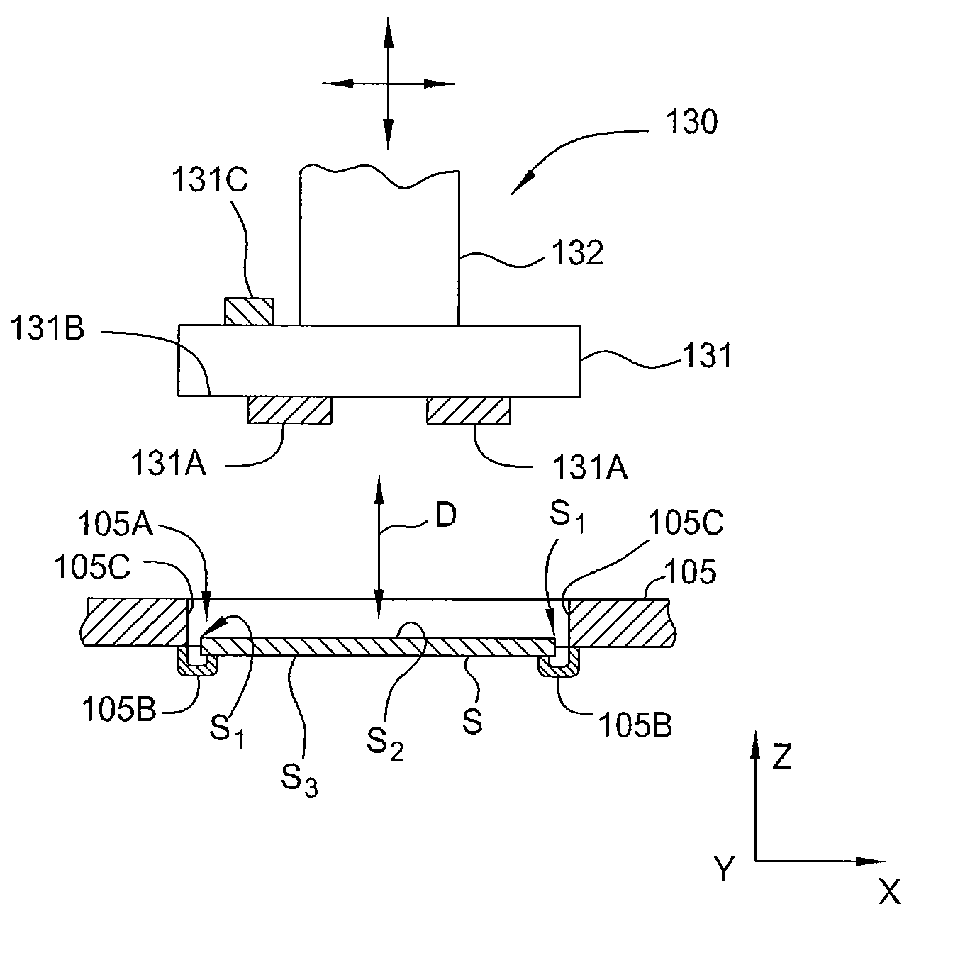
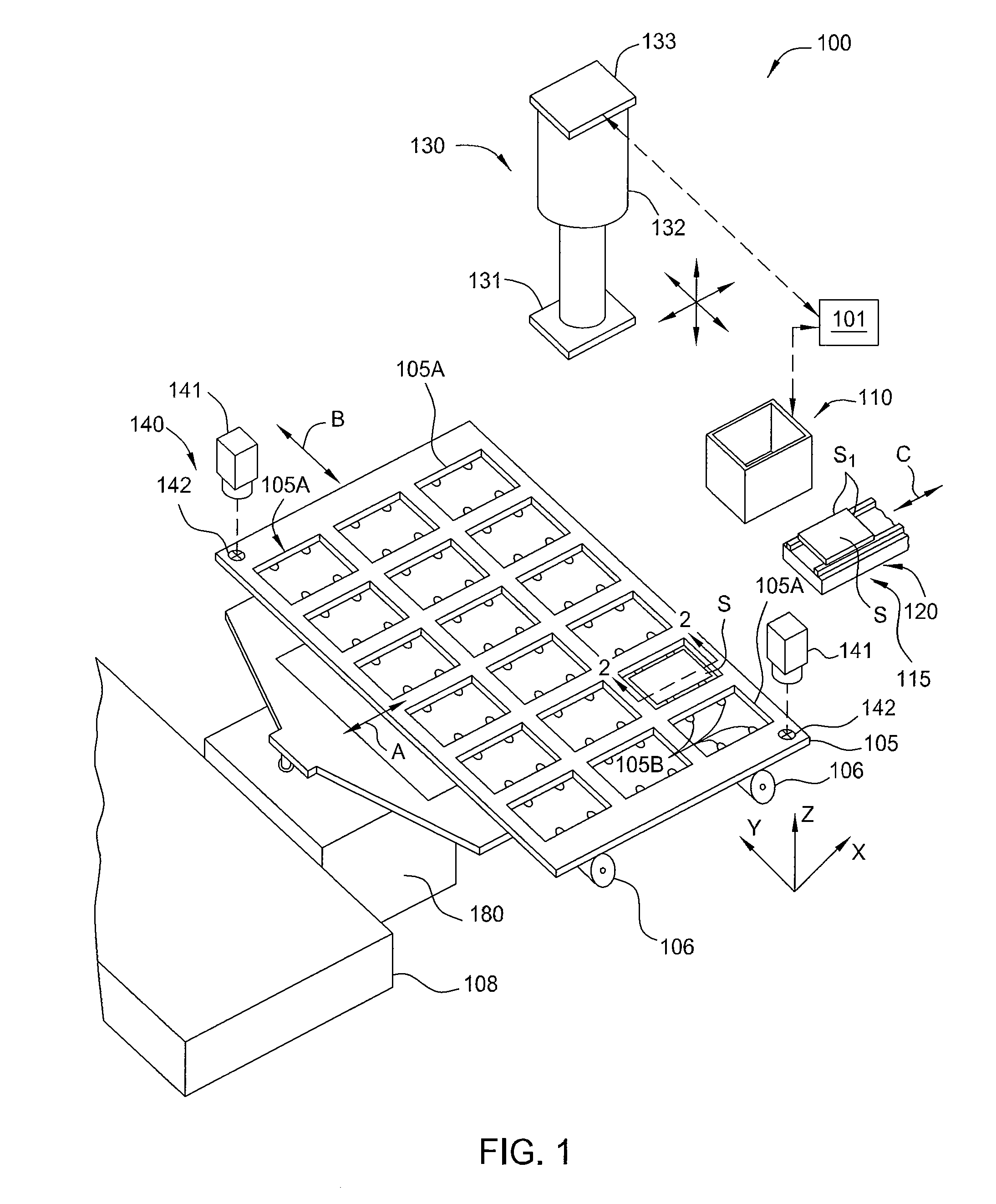
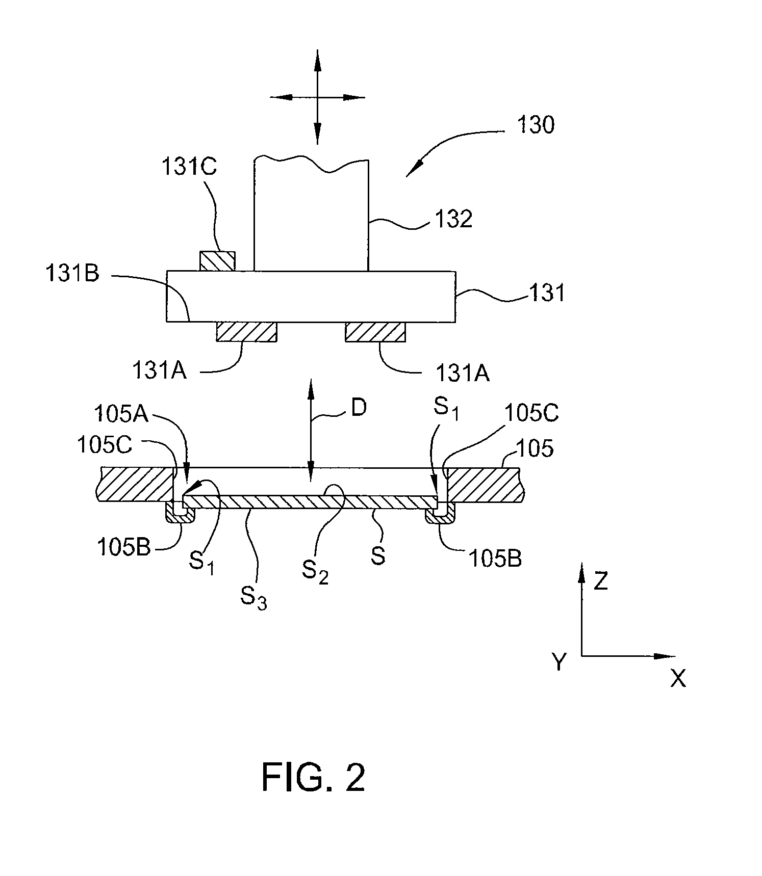
[0021]The present invention generally provides an apparatus and a method for automatically calibrating the placement of fragile substrates into a substrate carrier. Embodiments of the present invention also provide an apparatus and a method for inspecting the fragile substrates prior to processing to prevent damaged substrates from being further processed or broken in subsequent transferring steps. Embodiments of the invention also generally provide an apparatus and a method for determining the alignment and orientation of substrates that are to be delivered into or removed from the substrate carrier. Embodiments of the invention further provide an apparatus and method for accurately positioning the substrate carrier for substrate loading. The substrate carrier is used to support a batch of substrates that are to be processed in a batch processing module. In one example, as shown in FIG. 1, a loading station 100, which is positioned adjacent to a processing module 108 (FIG. 1), is c...


PUM


Abstract

The present invention generally provides an apparatus and a method for automatically calibrating the placement of fragile substrates into a substrate carrier. Embodiments of the present invention also provide an apparatus and a method for inspecting the fragile substrates prior to processing to prevent damaged substrates from being further processed or broken in subsequent transferring steps. Embodiments of the invention also generally provide an apparatus and a method for determining the alignment and orientation substrates that are to be delivered into or removed from a substrate carrier. Embodiments of the invention further provide an apparatus and method for accurately positioning the substrate carrier for substrate loading. The substrate carriers are generally used to support a batch of substrates that are to be processed in a batch processing chamber.

Description

CROSS-REFERENCE TO RELATED APPLICATIONS[0001]This application claims benefit of U.S. Provisional Patent Application Ser. No. 61 / 173,899 (APPM / 014355L), filed Apr. 29, 2009, which is herein incorporated by reference.BACKGROUND OF THE INVENTION[0002]1. Field of the Invention[0003]Embodiments of the invention generally relate to an apparatus and method for forming a solar cell device. The invention is particularly useful for fabrication of crystalline silicon solar cells.[0004]2. Description of the Related Art[0005]Photovoltaics (PV) or solar cells are devices which convert sunlight into direct current (DC) electrical power. A typical PV cell includes a p-type silicon wafer, substrate, or sheet typically less than about 0.3 mm thick with a thin layer of an n-type silicon material disposed on top of the p-type substrate. The generated voltage, or photo-voltage, and generated current by the photovoltaic device are dependent on the material properties of the p-n junction, the interfacial ...

Claims


Application Information

Patent Timeline
Patent Type & Authority Applications(United States)
IPC IPC(8): H01L21/66H04N7/18
CPCH01L21/67259H01L21/67155
Inventor SHAH, VINAY K.KUMARASWAMI, SURESHCOX, DAMON K.
Owner APPLIED MATERIALS INC
Why Eureka
Try Eureka