Semiconductor Memory Device

a memory device and semiconductor technology, applied in the field of semiconductor memory devices, can solve the problems of product yield suffer, memory device may not normally perform the desired operation, memory cell defects occur in a very small number of memory cells, etc., and achieve the effect of sufficient capacitance of redundancy memory cells

Active Publication Date: 2010-11-18
SK HYNIX INC
View PDF4 Cites 12 Cited by
  • Summary
  • Abstract
  • Description
  • Claims
  • Application Information

AI Technical Summary

Benefits of technology

[0024]An embodiment of the present invention is directed to providing a semiconductor memory device capable of ensuring relatively sufficient capacitance of a redundancy memory cell.

Problems solved by technology

If a fail occurs in a memory cell in a semiconductor memory device, the semiconductor memory device may not normally perform a desired operation.
As the fabrication technology of semiconductor memory devices has been advanced, defects occur in a very small number of memory cells.
Thus, if semiconductor memory devices are discarded as defective items when defects occur in few memory cells, product yield suffers.
Thus, noise occurring in the bit line is different from noise occurring in the complementary bit line, and the open bit line architecture is vulnerable to noises.
However, this approach is not suitable because such a design will increase the size of the semiconductor memory device.

Method used


Image

  • Semiconductor Memory Device
  • Semiconductor Memory Device
  • Semiconductor Memory Device

Examples


Embodiment Construction

[0033]Other objects and advantages of the present invention can be understood by the following description, and become apparent with reference to the embodiments of the present invention.

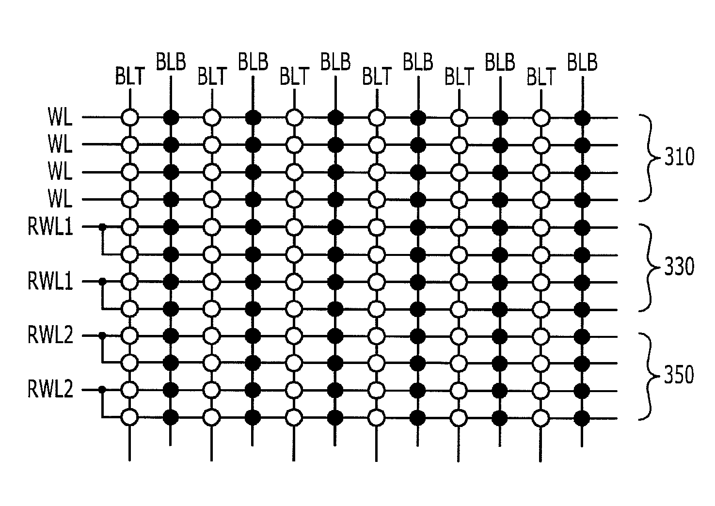
[0034]FIG. 3 illustrates a memory cell architecture of a semiconductor memory device in accordance with an embodiment of the present invention.

[0035]Referring to FIG. 3, the semiconductor memory device includes a normal memory cell array 310, a first redundancy memory cell array 330, and a second redundancy memory cell array 350. The normal memory cell array 310 and the first redundancy memory cell array 330 are designed within one memory cell mat, and the second redundancy memory cell array 350 is designed separately from the memory cell mat.

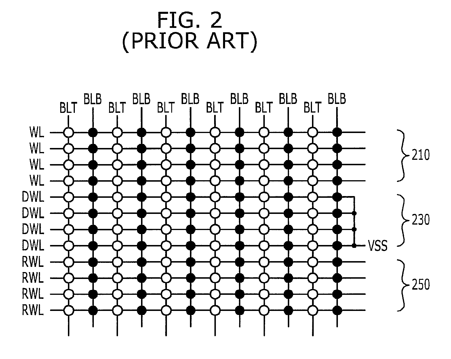
[0036]Compared with the conventional semiconductor memory device of FIG. 2, the architecture of the semiconductor memory device of FIG. 3 has at least the following two additional features.

[0037]First, in the conventional redundancy memory cell array 250 of FIG...


PUM


Abstract

A semiconductor memory device includes a plurality of memory cell mats each comprising a plurality of normal memory cell arrays; and a redundancy memory cell array configured to replace a defective memory cell with a plurality of redundancy memory cells corresponding to a redundancy word line when the redundancy word line corresponding to one or more redundancy memory cell arrays is activated in response to an address corresponding to the defective memory cell among the plurality of normal memory cell arrays.

Description

CROSS-REFERENCE TO RELATED APPLICATIONS[0001]The present invention claims priority of Korean Patent Application No. 10-2009-0041593, filed on May 13, 2009, the disclosure of which is incorporated herein by reference in its entirety.BACKGROUND OF THE INVENTION[0002]The present invention relates to a semiconductor design technology, and more particularly, to a semiconductor memory device that performs a data access operation by replacing a defective memory cell with a normal redundancy memory cell.[0003]With rapid increase in integration density of semiconductor memory devices including double data rate (DDR) synchronous dynamic random access memory (SDRAM), tens of millions of memory cells are integrated into a single semiconductor memory device. Such memory cells constitute memory cell arrays arranged uniformly, and those groups are called a memory cell mat.[0004]If a fail occurs in a memory cell in a semiconductor memory device, the semiconductor memory device may not normally perf...

Claims


Application Information

Patent Timeline
Patent Type & Authority Applications(United States)
IPC IPC(8): G11C29/00G11C8/00
CPCG11C29/816G11C8/08G11C29/00
Inventor KYUNG, KI-MYUNG
Owner SK HYNIX INC
Why Eureka
Try Eureka