Method of manufacturing carbon nanotube device array

a technology of carbon nanotubes and device arrays, which is applied in the direction of aligned nanotubes, instruments, photomechanical equipment, etc., can solve the problems of inefficiency in cost and/or time, and difficulty in mass production of cnt device arrays, so as to achieve easy and economical manufacturing and large area

Active Publication Date: 2010-11-18
SAMSUNG ELECTRONICS CO LTD
View PDF7 Cites 2 Cited by
  • Summary
  • Abstract
  • Description
  • Claims
  • Application Information

AI Technical Summary

Benefits of technology

[0015]According to example embodiments, a photolithography process may be used in the method of manufacturing the CNT device arrays so that CNTs may be formed on desired positions and the electrodes may be accurately formed on desired positions of the CNTs. Accordingly, CNT device arrays having a relatively large area may be more easily and economically manufactured. In addition, a plurality of electrodes may be formed on a single CNT so that a plurality of CNT devices having the same characteristics may be manufactured.

Problems solved by technology

However, the method of manufacturing CNT device arrays using e-beam lithography may be inefficient in terms of cost and / or time, and thus, mass production of the CNT device arrays may be difficult.

Method used


Image

  • Method of manufacturing carbon nanotube device array
  • Method of manufacturing carbon nanotube device array
  • Method of manufacturing carbon nanotube device array

Examples


Embodiment Construction

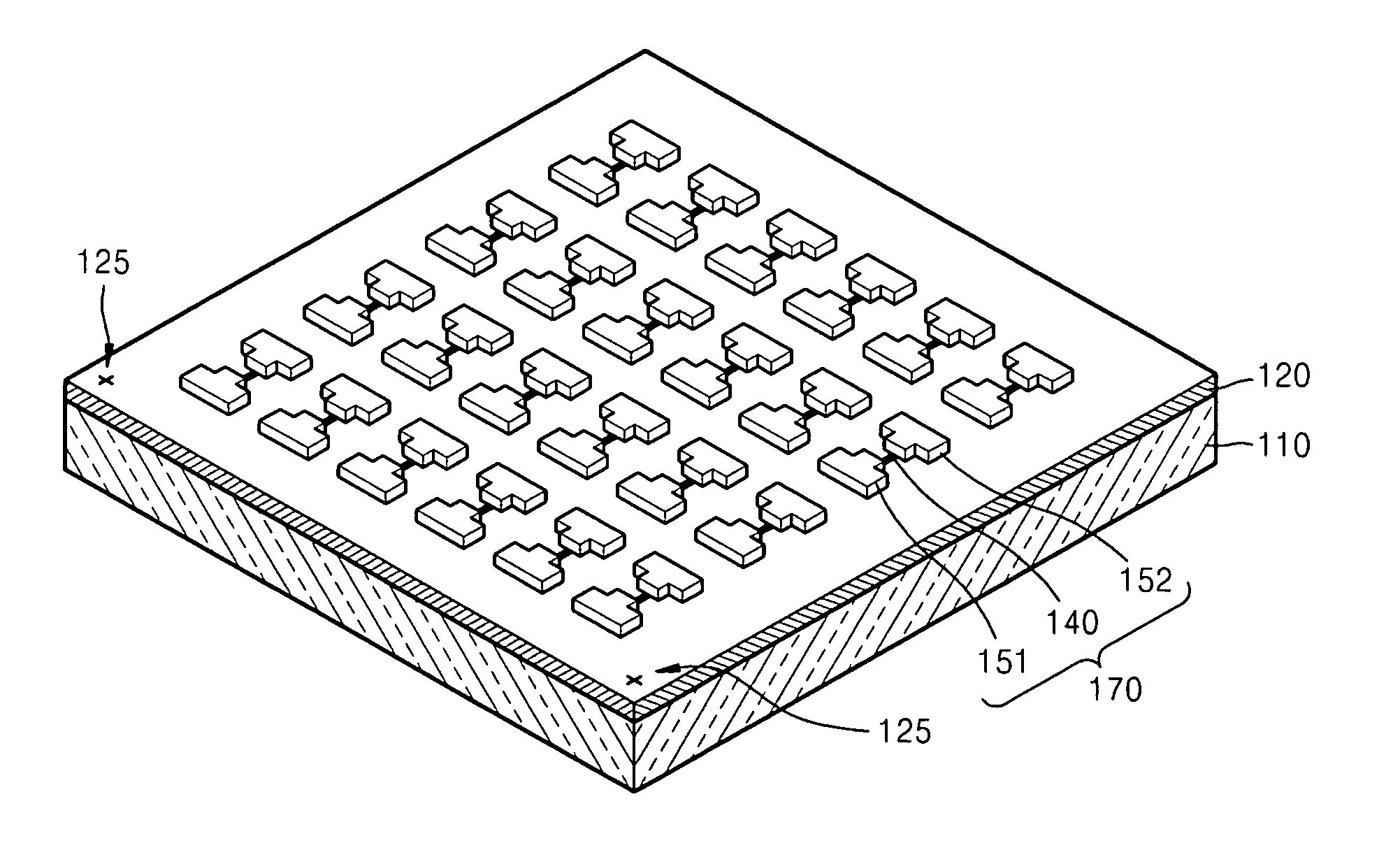
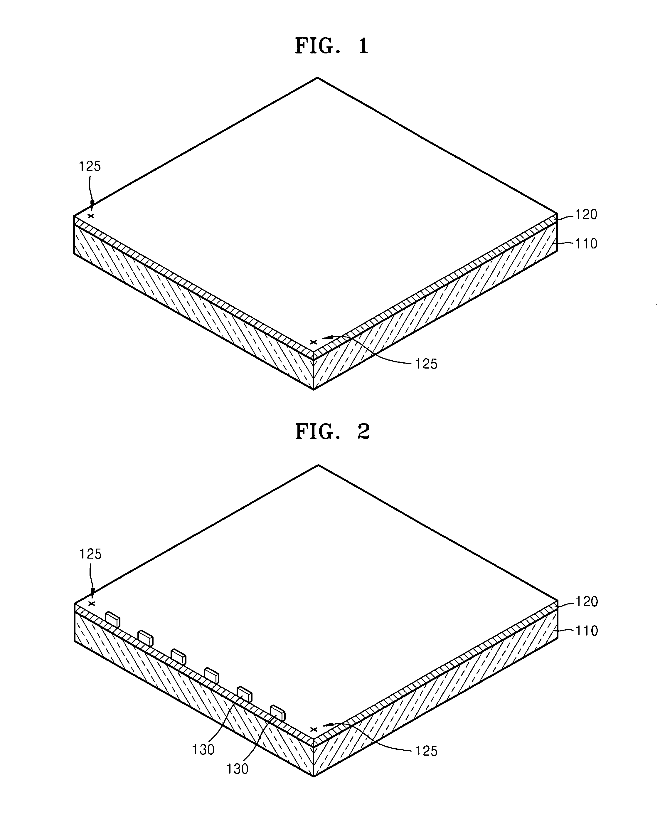
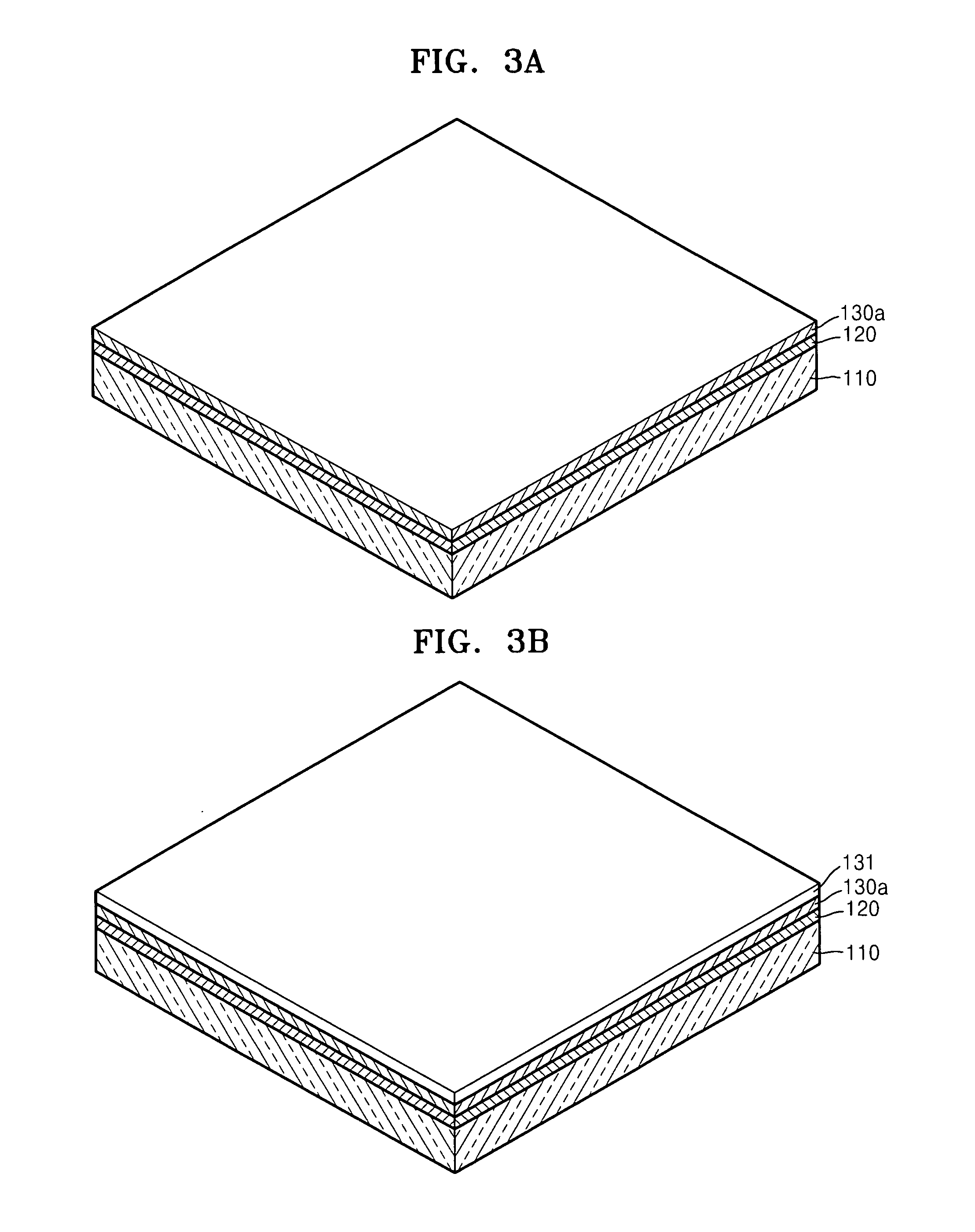
[0018]Hereinafter, example embodiments will be described more fully with reference to the accompanying drawings. However, specific structural and functional details disclosed herein are merely representative for purposes of describing example embodiments. In this regard, example embodiments may be embodied in many alternate forms and should not be construed as limited to only example embodiments set forth herein. In the drawings, like reference numerals denote like elements and the thicknesses of layers and regions are exaggerated for clarity.

[0019]Accordingly, while example embodiments are capable of various modifications and alternative forms, embodiments thereof are shown by way of example in the drawings and will herein be described in detail. It should be understood, however, that there is no intent to limit example embodiments to the particular forms disclosed, but on the contrary, example embodiments are to cover all modifications, equivalents, and alternatives falling within...


PUM

PropertyMeasurementUnit
shapeaaaaaaaaaa
atomic force microscopyaaaaaaaaaa
AFMaaaaaaaaaa

Abstract

Provided is a method of manufacturing carbon nanotube (CNT) device arrays. In the method of manufacturing CNT device arrays, catalyst patterns may be formed using a photolithography process, CNTs may be grown from the catalyst patterns, and electrodes may be formed on the grown CNTs.

Description

CROSS-REFERENCE TO RELATED APPLICATION[0001]This application claims priority under 35 USC §119 to Korean Patent Application No. 10-2009-0042192, filed on May 14, 2009, in the Korean Intellectual Property Office (KIPO), the entire contents of which are incorporated herein by reference.BACKGROUND[0002]1. Field[0003]Example embodiments relate to a method of manufacturing carbon nanotube (CNT) device arrays.[0004]2. Description of the Related Art[0005]Carbon nanotube (CNT) devices including CNTs may be formed in an array form and may be used to form various highly efficient electronic devices. For example, CNT device arrays may be used as efficient electronic devices in various areas, for example, logic circuits including complementary metal-oxide semiconductor (CMOS)-type inverters, memory devices including ring oscillators, static random access memories (SRAMs), non-volatile random access memories (NVRAMs), and other various sensors.[0006]CNT device arrays may be manufactured using e-...

Claims


Application Information

Patent Timeline
Patent Type & Authority Applications(United States)
IPC IPC(8): G03F7/20
CPCB82Y30/00C01B2202/08C01B31/0226B82Y40/00C01B32/16B82B3/00H01L21/0332
Inventor KIM, UN-JEONGLEE, EUN-HONGLEE, YOUNG-HEELEE, IL-HA
Owner SAMSUNG ELECTRONICS CO LTD
Why Eureka
Try Eureka