Liquid crystal display device

Active Publication Date: 2010-11-25
TRIVALE TECH
View PDF7 Cites 20 Cited by
  • Summary
  • Abstract
  • Description
  • Claims
  • Application Information

AI Technical Summary

Benefits of technology

[0014]The present invention has a superior advantage that can provide a liquid

Problems solved by technology

A conventional liquid crystal driving system, TN (Twisted Nematic) mode, is a system that changes a display state by applying a vertical electric field perpendicular to a substrate, raising o

Method used


Image

  • Liquid crystal display device
  • Liquid crystal display device
  • Liquid crystal display device

Examples


Example

First Exemplary Embodiment

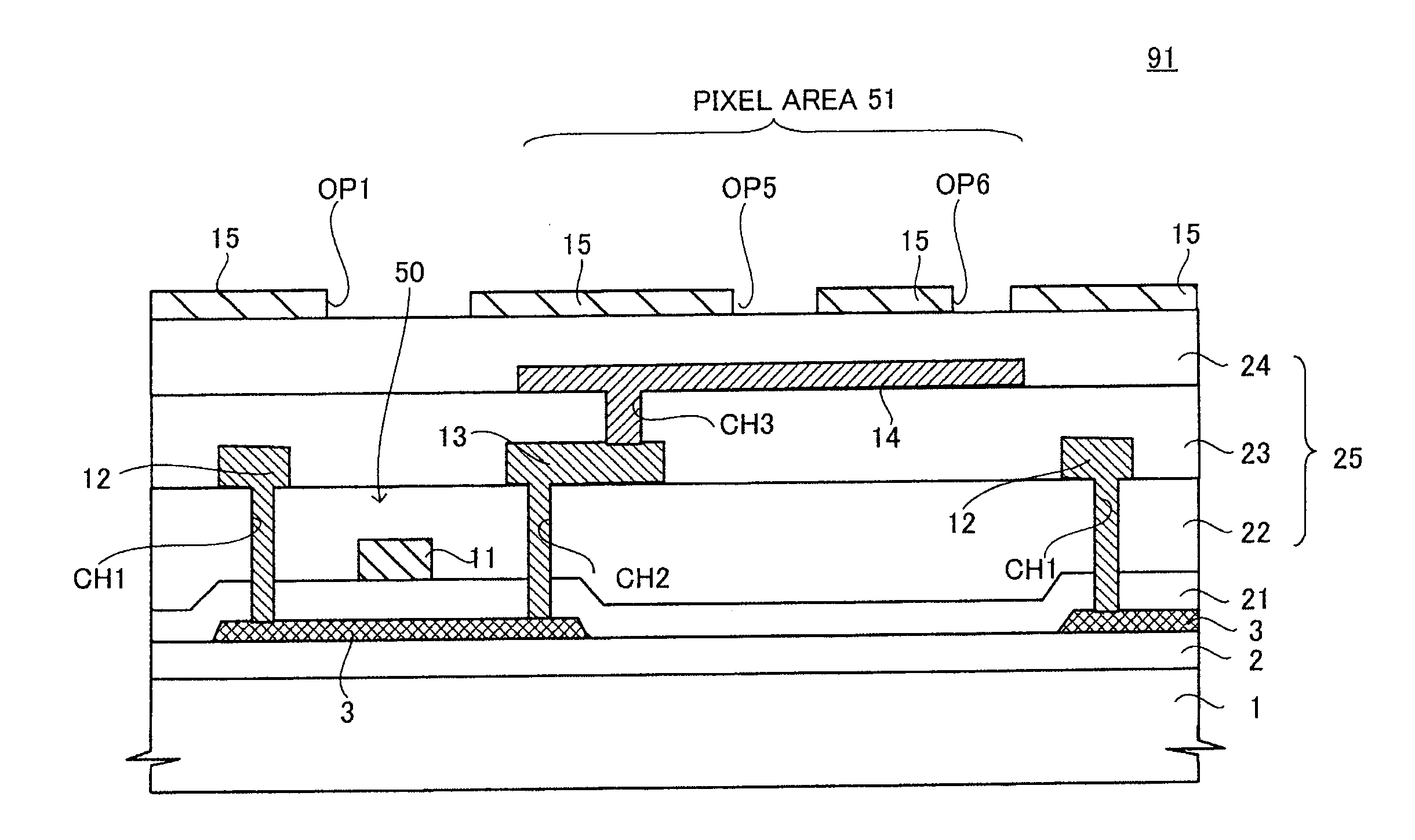
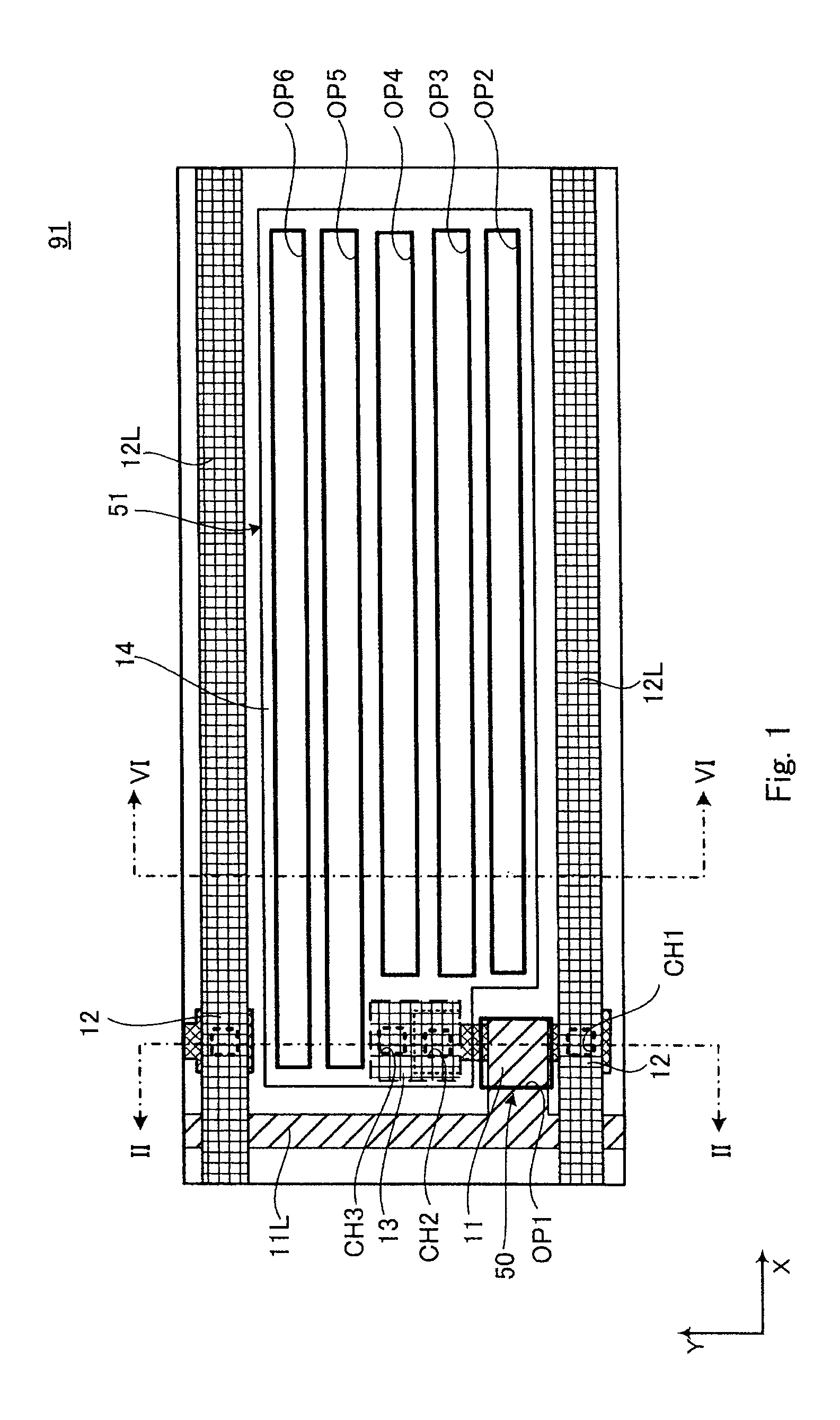
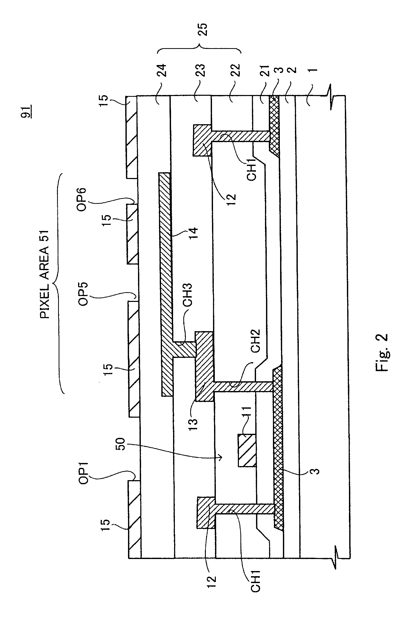
[0030]A liquid crystal display device in accordance with a first exemplary embodiment is a liquid crystal display device in the FFS mode provided with an active matrix type TFT array substrate that has a thin film transistor (TFT) of a top gate type MOS structure as a switching element. Here, a transmission type liquid crystal display device will be explained.

[0031]FIG. 1 is a schematic plan view showing an enlarged partial TFT array substrate that works as a first substrate mounted in the liquid crystal display device in accordance with the first exemplary embodiment, and FIG. 2 is a sectional view taken from a line II-II of FIG. 1. It is to be noted that for the purpose of explanation, in FIG. 1, a gate insulating film, an insulating layer (a first interlayer insulating film, a second interlayer insulating film, and a third interlayer insulating film), slit electrodes, etc are omitted. Meanwhile, positions of pattern apertures are shown in FIG. 1 in term...

Example

Second Exemplary Embodiment

[0076]Next, an example of a liquid crystal display panel different from the above-described first exemplary embodiment is described. In the drawings described below, the same component members as in the above-described first exemplary embodiment have the same reference numerals, and explanations thereof are arbitrarily omitted.

[0077]In FIG. 8, shown is a schematic enlarged partial sectional view of the liquid crystal display panel 90 in accordance with a second exemplary embodiment. In the second exemplary embodiment, various values are set so as to meet the following conditions.

w3

[0078]Namely, a width w3 of an N-slit electrode 15Ba adjacent to an S-slit electrode 15Aa is set to be smaller than a width w4 of the E-slit electrodes 15C other than the S-slit electrode 15Aa and the N-slit electrode 15Ba. Simultaneously, the width of both ends of the S-slit electrode 15Aa is set to be larger by a width w5 than that of the comparative example. Specifically, whe...

Example

Third Exemplary Embodiment

[0084]Next, an example of a liquid crystal display panel different from the above-described second exemplary embodiment is described. In a third exemplary embodiment, various values are set so as to meet the following conditions.

[0085]In FIG. 11, shown is a transmittance distribution graph in an area corresponding to the line VI-VI of the first exemplary embodiment in the liquid crystal display panel in accordance with the third exemplary embodiment.

wS1

[0086]Namely, a width wS1 of the slit-like aperture OP between an S-slit electrode 15Ab and an N-slit electrode 15Bb is set to be smaller than a width wS2 of the slit-like aperture OP between the N-slit electrode 15Bb and the E-slit electrode 15C, and of the slit-like aperture OP between the E-slit electrodes 15C. Simultaneously, the width of both ends of the S-slit electrode 15Ab is set to be larger than that of the comparative example. Specifically, when a size of one pixel is set to 43.5 μm×130.5 μm, wS2 ...


PUM


Abstract

A liquid crystal device according to an embodiment of the present invention includes: a first substrate including a slit electrode that has slit-like apertures to form line-like patterns substantially in a same direction as either source wires or gate wires; a second substrate including a light shielding film that extends in a same direction as the line-like patterns of the slit electrode, and that has an overlap area with either the source wires or the gate wires, and that is arranged that color filter films are partitioned to prevent color mixture when displayed in a single color. A non-opposed area to the light shielding film is formed at an end of the slit electrode in a width direction that a transmittance may not be reduced due to the light shielding film in the areas where the light shielding film and the slit electrode are arranged in an overlapped manner.

Description

INCORPORATION BY REFERENCE[0001]This application is based upon and claims the benefit of priority from Japanese patent application No. 2009-121667, filed on May 20, 2009, the disclosure of which is incorporated herein in its entirety by reference.BACKGROUND OF THE INVENTION[0002]1. Field of the Invention[0003]The present invention relates to a liquid crystal display device and, more particularly, to a liquid crystal display device in the FFS (Fringe Field Switching) mode.[0004]2. Description of Related Art[0005]A liquid crystal display device is one of flat panels, and it is widely used in monitors of personal computers and portable information terminal devices, etc., by taking advantage of its low power consumption, compactness, and lightweight. In addition, the liquid crystal display device is also widely used for TV sets, and it is replacing conventional cathode-ray tubes.[0006]A mainstream of the liquid crystal display device in recent years is an active matrix type in which a p...

Claims


Application Information

Patent Timeline
IPC IPC(8): G02F1/1343
CPCG02F1/134363G02F1/133512
Inventor YONEMURA, KOJI
Owner TRIVALE TECH
Why Eureka
Try Eureka