Electrostatic discharge clamp circuit

a clamp circuit and electrostatic discharge technology, applied in the direction of emergency protective circuit arrangements, emergency protective arrangements for limiting excess voltage/current, emergency protective arrangements, etc., can solve the problems of permanent damage, esd, and damage to the function of electronic devices, so as to reduce the circuit layout area and extend the turn-on time of the clamp

Active Publication Date: 2010-11-25
IND TECH RES INST
View PDF15 Cites 38 Cited by
  • Summary
  • Abstract
  • Description
  • Claims
  • Application Information

AI Technical Summary

Benefits of technology

[0010]The present disclosure is directed to an electrostatic discharge (ESD) clamp circuit, which utilizes a parasitic capacitor of a clamp device to implement a detection circuit, and extends a turn-on time of the clamp device by a control circuit with a feedback scheme, so as to decrease a circuit layout area.
[0012]When an ESD occurs, the first transistor is turned on by utilizing a parasitic capacitor of the third transistor and the second resistor. The current generated after the first transistor is turned on flows through the first resistor, so as to generate a voltage drop to turn on the second transistor. The current generated by turning on the second transistor increases the voltage applied to turn on the first transistor and the third transistor through the second resistor. With such a feedback scheme, the voltage for turning on the third transistor is increased, the third transistor is turned on to discharge the ESD current during the ESD, and the channel turn-on time of the third transistor depends on the length of time that the ESD lasts. Meanwhile, such an ESD clamp circuit requires only a few of devices to implement, and can reduce the circuit layout area.

Problems solved by technology

Electronic devices are often suffered from electrostatic discharge (ESD).
Because the voltage generated by the ESD event is much higher than the voltage that the electronic devices can endure, the function of the electronic devices may be damaged, or even permanent damage is caused.
Moreover, the electronic devices themselves may also accumulate static electricity, and the static electricity can be discharged while the electronic devices are grounded during assembling, thus resulting in unexpected loss.
However, the RC circuit having overly large resistance value and capacitance value may result in the problem that the ESD clamp circuits 100 and 110 are liable to be triggered wrongly when they are suffering from large noises.
Meanwhile, a quite large layout area is required when the RC circuit having overly large resistance value and capacitance value is applied in circuit layout.
However, the manner may increase the risk of being wrongly triggered when the circuit is in a fast power-on, and may occupy a large layout area.
In addition, utilizing a control circuit having a feedback scheme to implement the clamp circuit still has the risk of being wrongly triggered due to overly large power noise.
Meanwhile, such an ESD clamp circuit requires only a few of devices to implement, and can reduce the circuit layout area.

Method used


Image

  • Electrostatic discharge clamp circuit
  • Electrostatic discharge clamp circuit
  • Electrostatic discharge clamp circuit

Examples


Embodiment Construction

[0034]Reference will now be made in detail to these embodiments of the invention, examples of-which are illustrated in the accompanying drawings. Wherever possible, the same reference numbers are used in the drawings and the description to refer to the same or like parts.

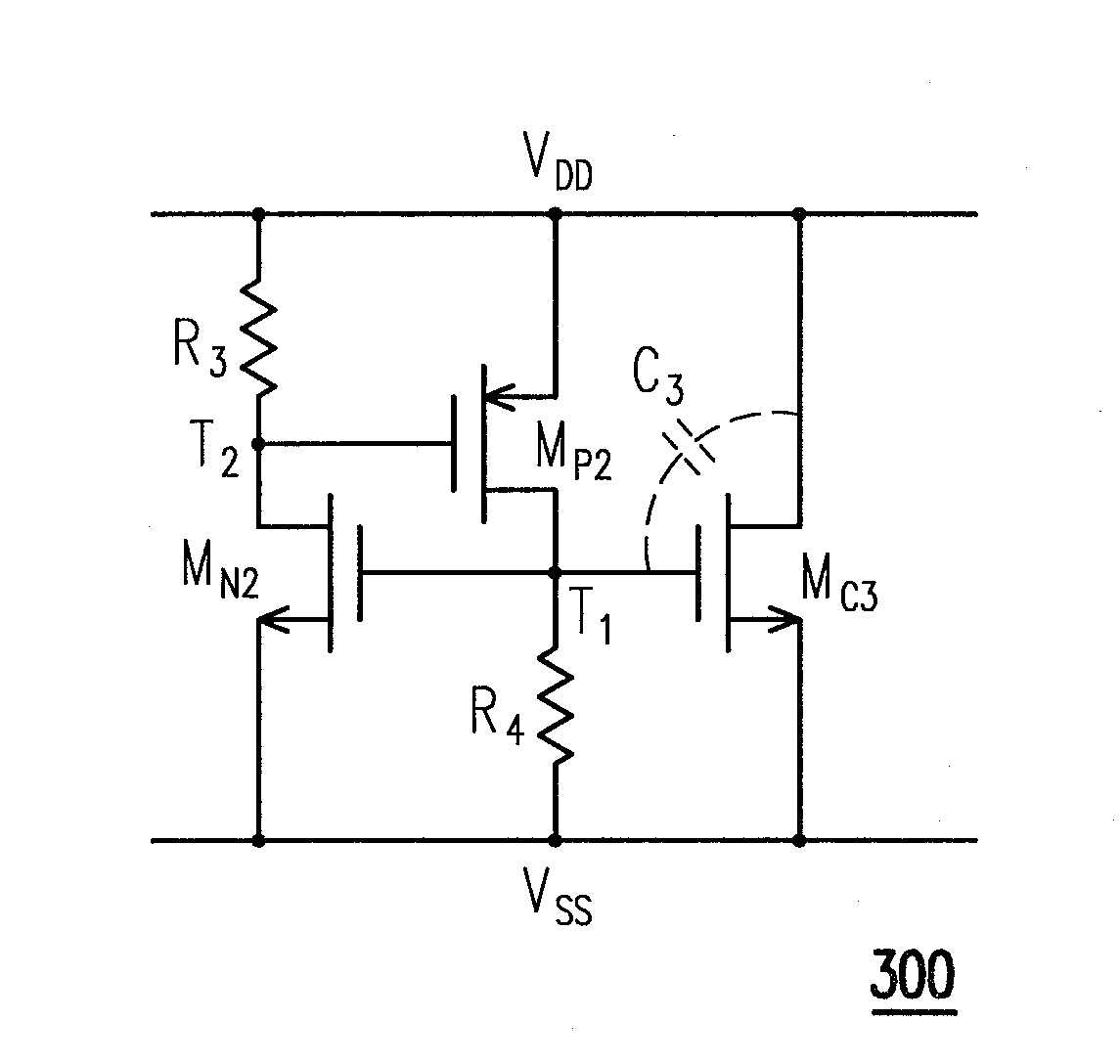
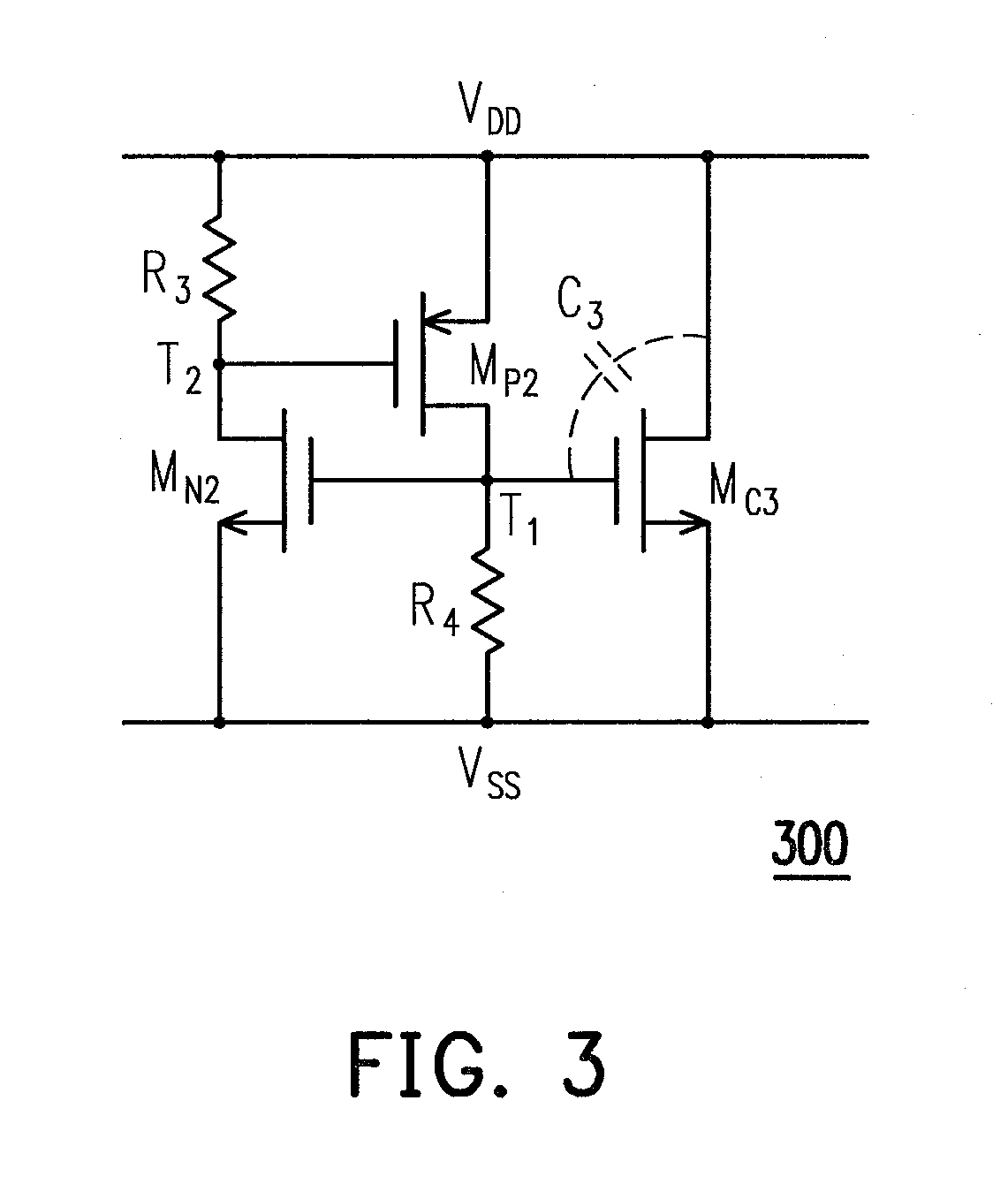
[0035]FIG. 3 is an electrostatic discharge (ESD) clamp circuit diagram according to an exemplary embodiment consistent with the present invention. Referring to FIG. 3, an ESD clamp circuit 300 includes a first resistor R3, a second resistor R4, a first transistor MN2, a second transistor MP2, and a third transistor MC3. In this embodiment, the first transistor MN2 is an NMOS transistor, the second transistor MP2 is a PMOS transistor, the third transistor MC3 is an n-channel big field effect transistor (BIGFET), but the present invention is not so limited. A first end of the resistor R3 is coupled to a first rail (for example, a power rail VDD), a second end of the resistor R4 is coupled to a second rail (for example...


PUM


Abstract

An electrostatic discharge (ESD) clamp circuit is provided. The ESD clamp circuit includes a first resistor, a second resistor, a first transistor, a second transistor, and a third transistor. A clamp device of the ESD clamp circuit is implemented by the third transistor. A parasitic capacitor of the third transistor forms a detection scheme along with the second resistor to detect the ESD. The first resistor, the second resistor, the first transistor, and the second transistor form a feedback scheme to control the third transistor for discharging the ESD current.

Description

CROSS-REFERENCE TO RELATED APPLICATION[0001]This application claims the priority benefit of Taiwan application serial no. 98116793, filed on May 20, 2009. The entirety of the above-mentioned patent application is hereby incorporated by reference herein and made a part of specification.BACKGROUND[0002]1. Technical Field[0003]The present disclosure generally relates to a protection circuit, in particular, to a protection circuit for electrostatic discharge.[0004]2. Description of Related Art[0005]With the progress of technology, electronic devices are displacing traditional mechanical devices gradually. Electronic devices are often suffered from electrostatic discharge (ESD). The static electricity accumulated in human body (or machine) may be discharged through the electronic devices because of human body (or machine) contact, whether in manufacturing process or in actual use. Because the voltage generated by the ESD event is much higher than the voltage that the electronic devices c...

Claims


Application Information

Patent Timeline
Patent Type & Authority Applications(United States)
IPC IPC(8): H02H9/04
CPCH01L27/0285H01L2924/0002H01L2924/00H02H9/046
Inventor LIANG, YUNG-CHIHYEH, CHIH-TINGCHEN, SHIH-HUNG
Owner IND TECH RES INST
Why Eureka
Try Eureka