
Optical filter, optical filter device, analyzer, and method for manufacturing optical filter

a technology of optical filter and analyzer, which is applied in the direction of optical elements, mountings, instruments, etc., to achieve the effect of accurate control

Inactive Publication Date: 2010-12-02
SEIKO EPSON CORP
View PDF21 Cites 33 Cited by
  • Summary
  • Abstract
  • Description
  • Claims
  • Application Information

AI Technical Summary

Benefits of technology

[0007]An advantage of some aspects of the invention is to provide an optical filter in which mirrors are prevented from being charged to thereby eliminate sticking of the mirrors together, an optical filter device, an analyzer, and a method for manufacturing an optical filter.

Problems solved by technology

However, when the substrates are bonded together by surface activated bonding, the mirrors are charged due to ion beam, plasma or an electrostatic chuck used for supporting the substrate, or the like, causing a problem in that the mirrors stick together by an electrostatic attraction caused by charges accumulating on the mirrors when the substrates are bonded together.

Method used


Image

  • Optical filter, optical filter device, analyzer, and method for manufacturing optical filter
  • Optical filter, optical filter device, analyzer, and method for manufacturing optical filter
  • Optical filter, optical filter device, analyzer, and method for manufacturing optical filter

Examples


first embodiment

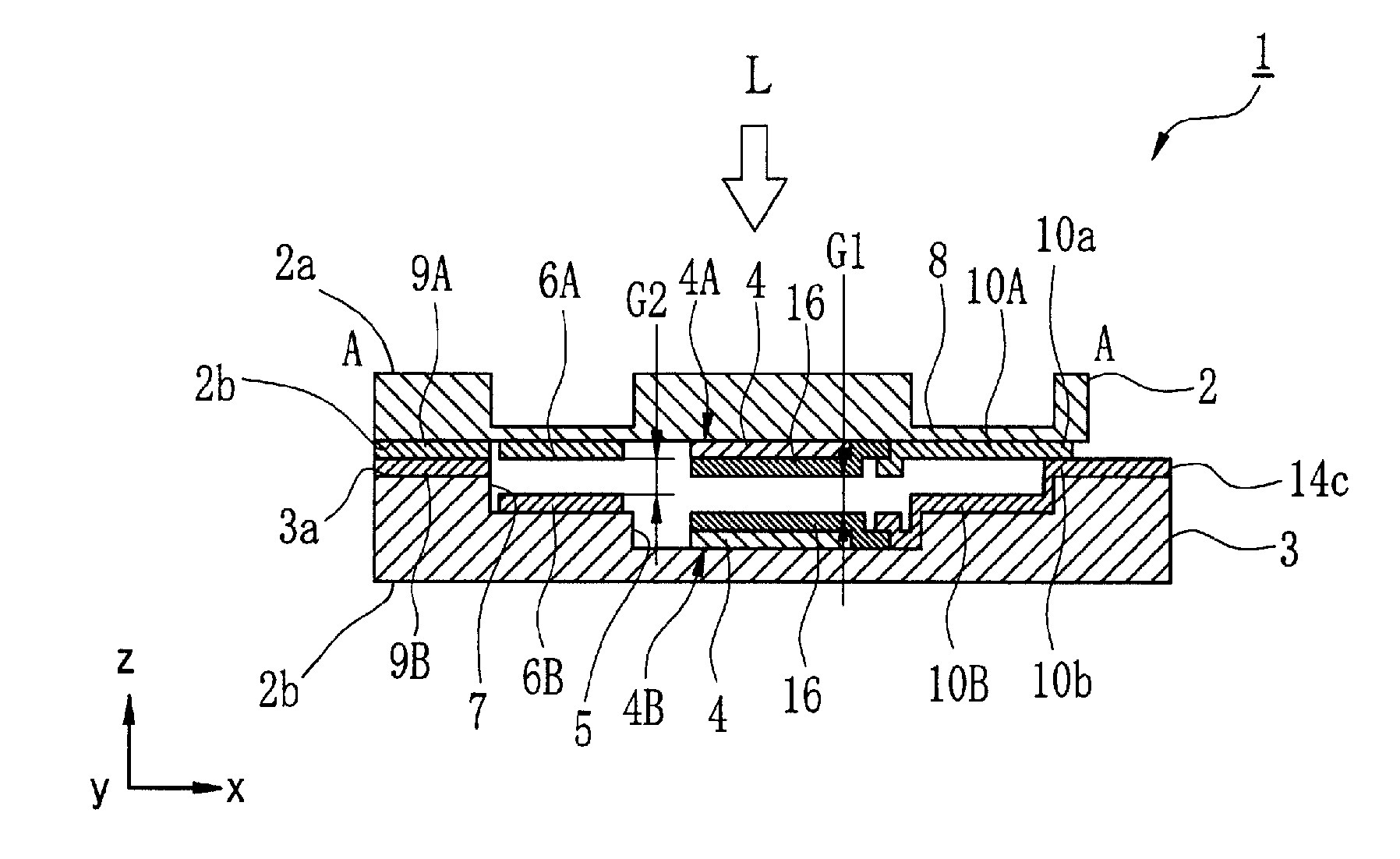
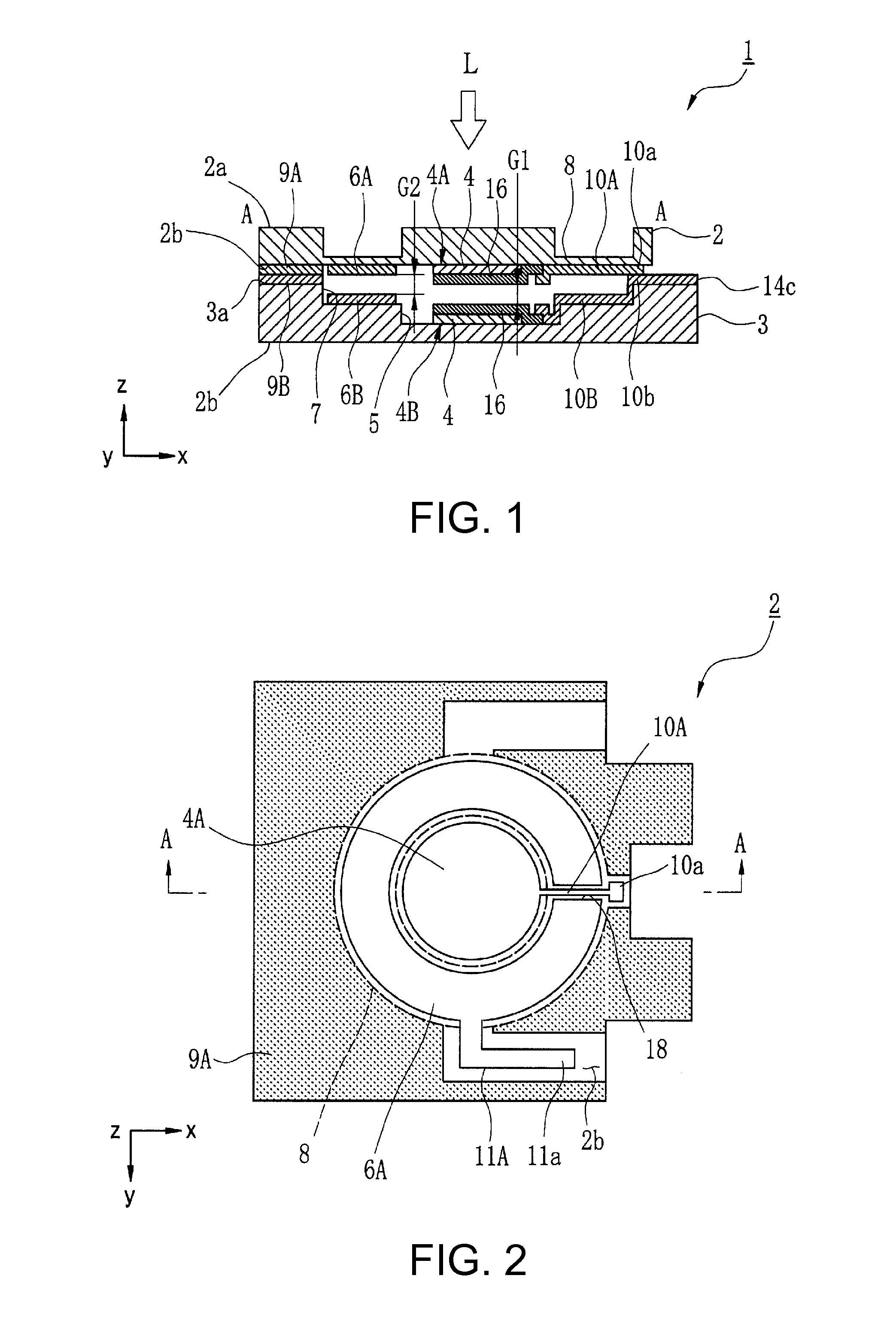
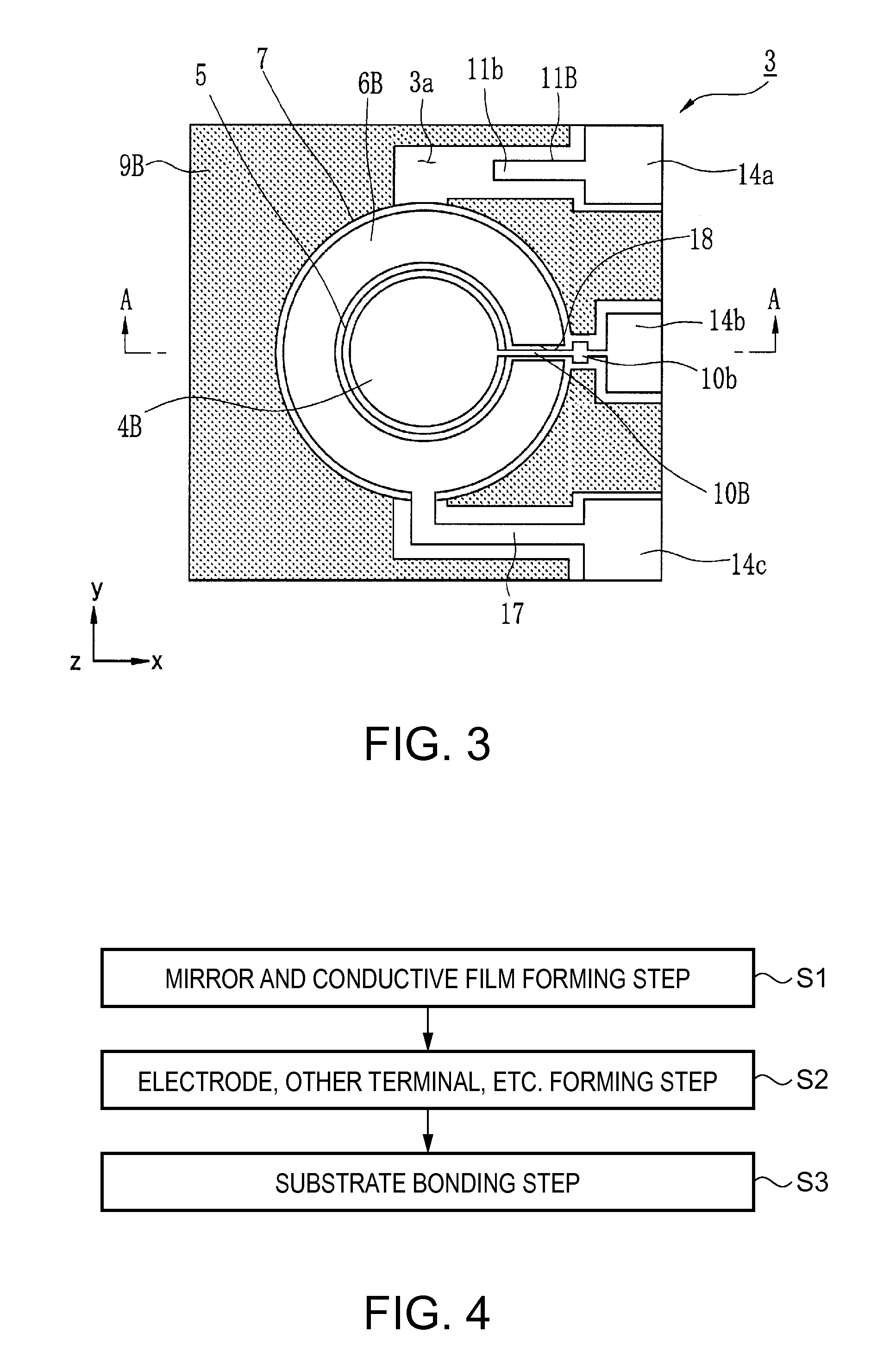
[0056]FIG. 1 is a cross-sectional view showing an optical filter as a first embodiment of the invention. FIG. 2 is a plan view of a first substrate 2 constituting the optical filter as viewed from a bonding surface 2b side. FIG. 3 is a plan view of a second substrate 3 constituting the optical filter as viewed from a bonding surface 3a side.

[0057]The optical filter 1 of the embodiment shown in FIGS. 1 to 3 is an electrostatically-driven airgap type etalon element.

[0058]The optical filter 1 includes the first substrate 2 and the second substrate 3 bonded to the first substrate 2 in a facing state.

[0059]As shown in FIGS. 1 and 2, on the first substrate 2, a mirror 4A (first mirror), an electrode 6A, a diaphragm portion 8, a bonding metal film 9A, a first wire 10A, and an inter-substrate conducting wire 11A are disposed. The mirror 4A is circular in a plane view and disposed at the central portion of the bonding surface 2b on the side facing the second substrate 3. The electrode 6A is ...

second embodiment

[0100]Next, a second embodiment of the invention will be described by using FIGS. 6 to 8. FIG. 6 is a cross-sectional view showing an optical filter of the second embodiment. FIG. 7 is a plan view of a first substrate constituting the optical filter of the second embodiment shown from a bonding surface side. FIG. 8 is a plan view of a second substrate shown from a bonding surface side.

[0101]The optical filter of the embodiment shown below is substantially similar to that of the aforementioned embodiment in basic configuration but is different in that the electrical conduction between the substrates is realized by bump connection. In the following description, therefore, a configuration different from that of the aforementioned embodiment will be described in detail, and the description for the common part is omitted. In the drawings used for the description, the common constituent elements with those in FIGS. 1 to 5D are denoted by the same reference numerals and signs.

[0102]As show...

third embodiment

[0107]Next, a third embodiment of the invention will be described by using FIGS. 9 and 10A and 10B. FIG. 9 is a cross-sectional view showing an optical filter of the third embodiment. FIG. 10A is a plan view of a first substrate constituting the optical filter of the third embodiment shown from a bonding surface side. FIG. 10B is a plan view of a second substrate shown from a bonding surface side.

[0108]As shown in FIG. 9, the optical filter of the embodiment is different from those of the aforementioned embodiments in that the mirrors 4A and 4B are insulated from each other in a completed state.

[0109]As shown in FIG. 9, the movable mirror 4A is connected to the electrode pad 14b on the second substrate 3 side via the bump connection portion 21 of the first wire 10A and the connection portion 10b of the second wire 10B. On the other hand, the first electrode 6A disposed on the first substrate 2 is connected to the electrode pad 14a on the second substrate 3 via the bump connection po...


PUM

PropertyMeasurementUnit
elastic bodyaaaaaaaaaa
conductiveaaaaaaaaaa
light-transmissive conductiveaaaaaaaaaa

Abstract

An optical filter includes: a first substrate and a second substrate that are disposed to face each other; a first mirror and a first electrode that are disposed on the second substrate side of the first substrate; and a second mirror and a second electrode that are disposed on the first substrate side of the second substrate, wherein the first mirror and the second mirror are connected via a wire.

Description

BACKGROUND[0001]1. Technical Field[0002]The present invention relates to an optical filter, an optical filter device, an analyzer, and a method for manufacturing an optical filter.[0003]2. Related Art[0004]As optical filters that select light having a wavelength as a target from incident light and allow the light to be emitted in the related art, an optical filter having a structure in which a pair of substrates are disposed to face each other, a mirror is disposed on each facing surface of the substrates, an electrode is disposed around each of the mirrors, and a diaphragm portion is disposed around at least one of the mirrors has been known. Such an optical filter can selectively extract light having a wavelength corresponding to the gap between the pair of facing mirrors. Voltage is applied to a fixed electrode disposed on one of the substrates and a movable electrode disposed on the other substrate, whereby the gap between the mirrors can be controlled to a desired value by elec...

Claims


Application Information

Patent Timeline
Patent Type & Authority Applications(United States)
IPC IPC(8): G02B5/08B32B38/00G02B1/10G02B1/16G02B26/00
CPCG01J3/26G01J3/42G01J3/51G02B26/001
Inventor HIROKUBO, NOZOMUFUNASAKA, TSUKASA
Owner SEIKO EPSON CORP
Learn More