

Clock switch circuit and clock switch method of the same
- Summary
- Abstract
- Description
- Claims
- Application Information
AI Technical Summary
Benefits of technology
Problems solved by technology
Method used
Image

Examples
first exemplary embodiment
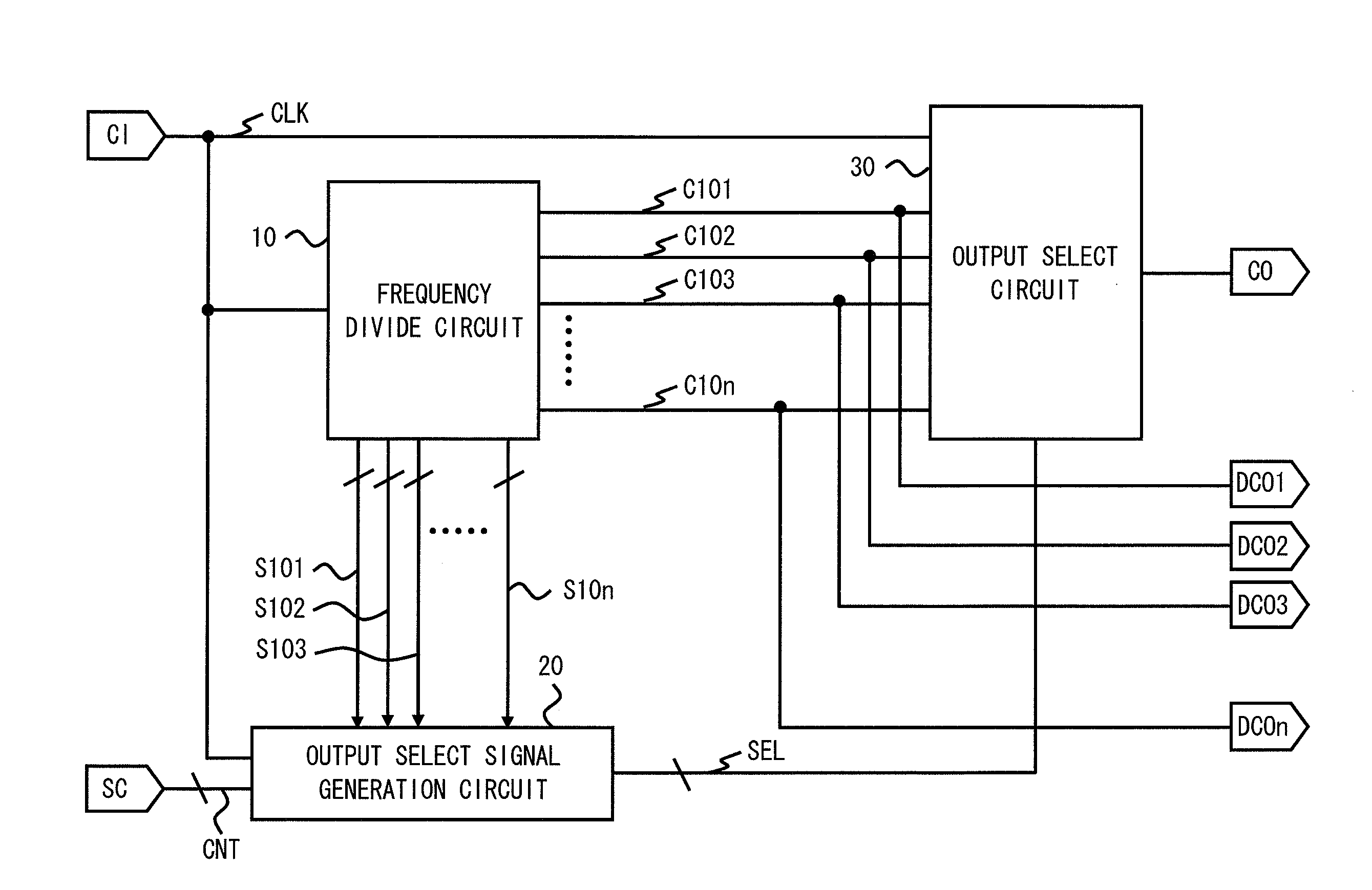
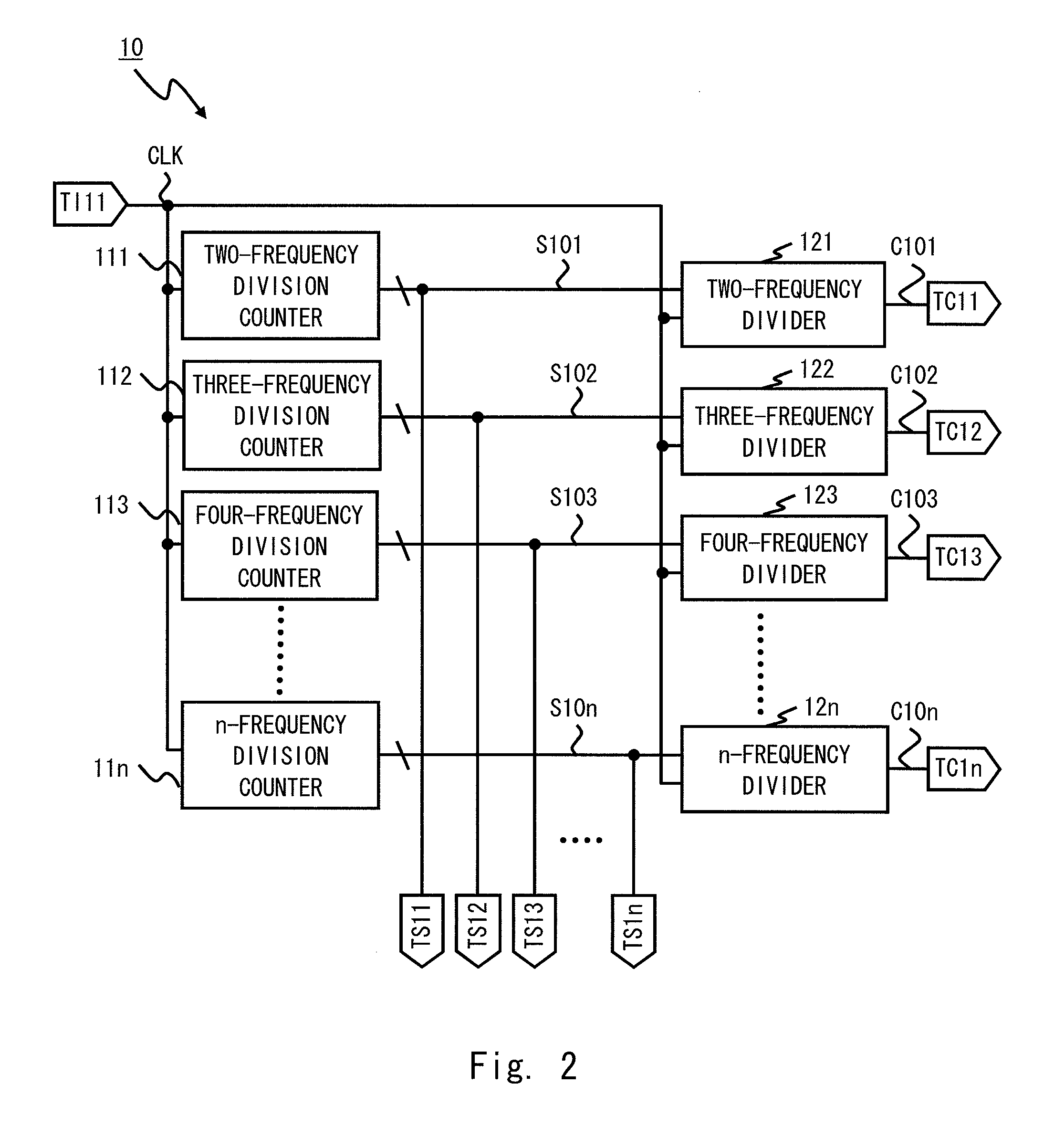
[0026]Hereinafter, specific exemplary embodiments of the present invention will be described with reference to the drawings. FIG. 1 shows a block diagram showing a clock switch circuit 1 according to a first exemplary embodiment. As shown in FIG. 1, the clock switch circuit 1 includes a frequency divide circuit 10, an output select signal generation circuit 20, and an output select circuit 30. The clock switch circuit 1 further includes input terminals CI, SC, and output terminals CO, DCO1 to DCOn. The input terminal CI is a terminal that inputs a basic clock CLK, the input terminal SC is a terminal that inputs a clock select signal CNT, the output terminal CO is a terminal which outputs an output signal OUT, and output terminals DCO1 to DCOn are output terminals which are provided corresponding to n (n is a positive integer indicating the number of frequency-divided clocks, hereinafter the same) frequency-divided clocks. These terminals are connected to other circuits that are not ...
second exemplary embodiment
[0046]FIG. 5 shows a block diagram of a clock switch circuit 2 according to a second exemplary embodiment. As shown in FIG. 5, the clock switch circuit 2 includes a frequency divide circuit 40 having a different form from that of the frequency divide circuit 10, and an output select signal generation circuit 50 having a different form from that of the output select signal generation circuit 20 of the clock switch circuit 1 according to the first exemplary embodiment. In the description of the clock switch circuit 2 according to the second exemplary embodiment, the same components as those of the clock switch circuit 1 according to the first exemplary embodiment will be denoted by the same reference symbols, and description thereof will be described.
[0047]The frequency divide circuit 40 generates a plurality of frequency-divided clocks based on the basic clock CLK and a plurality of frequency-divided count values corresponding to the plurality of frequency-divided clocks. The frequen...
third exemplary embodiment
[0068]A clock switch circuit according to a third exemplary embodiment has a form different from that of the reset signal generation circuit 60 according to the second exemplary embodiment. The whole block diagram of the clock switch circuit according to the third exemplary embodiment is similar to that of the clock switch circuit 2 shown in FIG. 5, and thus description will be omitted. FIG. 10 shows a block diagram of an output select signal generation circuit 50a including a reset signal generation circuit 80 having a form different from that of the reset signal generation circuit 60. In the description of the clock switch circuit according to the third exemplary embodiment, the same components as those of the clock switch circuits in the first and second exemplary embodiments are denoted by the same reference symbols, and description thereof will be omitted.
[0069]As shown in FIG. 10, the output select signal generation circuit 50a includes a reset signal generation circuit 80 in ...
PUM
 Abstract
Description
Claims
Application Information