

ESD protection device
a protection device and protection device technology, applied in the direction of emergency protective arrangements for limiting excess voltage/current, spark gap details, circuit arrangements, etc., can solve the problem of reducing the variation in the responsiveness to esd, and achieve the effect of high precision, easy adjustment and stabilization, and reduced characteristic variation such as the starting voltage of the discharg
- Summary
- Abstract
- Description
- Claims
- Application Information
AI Technical Summary
Benefits of technology
Problems solved by technology
Method used
Image

Examples
example 1
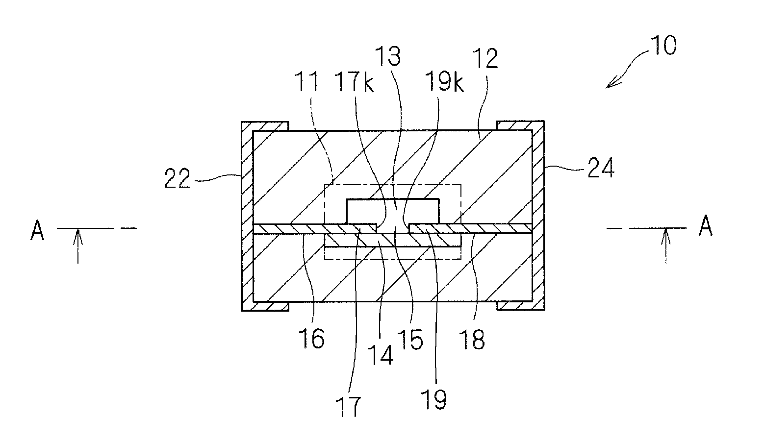
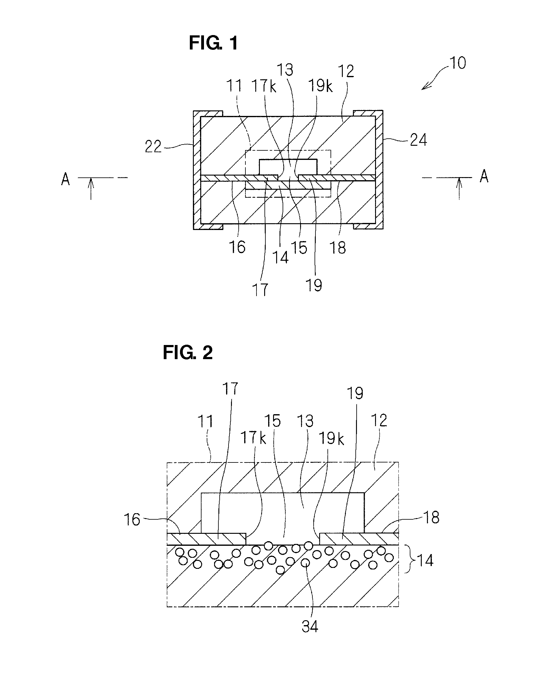
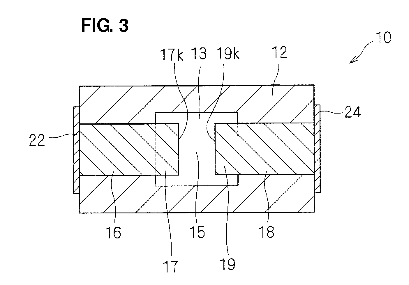
[0040]An ESD protection device 10 of Example 1 is described with reference to FIGS. 1 to 4. FIG. 1 is a sectional view of the ESD protection device 10. FIG. 2 is an enlarged sectional view of a principal portion schematically showing a region 11 indicated by a chain line in FIG. 1. FIG. 3 is a sectional view taken along line A-A of FIG. 1.
[0041]As shown in FIG. 1, the ESD protection device 10 includes a cavity 13 and a pair of discharge electrodes 16 and in a ceramic multilayer substrate 12. The discharge electrodes 16 and 18 respectively include counter portions 17 and 19 arranged along the inner surface of the cavity 13. The discharge electrodes 16 and 18 extend from the cavity 13 to the outer surface of the ceramic multilayer substrate 12, and are respectively connected to external electrodes 22 and 24 located outside of the ceramic multilayer substrate 12, that is, on the surface of the ceramic multilayer substrate 12. The external electrodes 22 and 24 are used for mounting the ...
example 2
[0090]An ESD protection device 10s of Example 2 will be described with reference to FIG. 8. FIG. 8 is a sectional view of the ESD protection device 10s.
[0091]The ESD protection device 10s of Example 2 has substantially the same structure as that of the ESD protection device 10 of Example 1. The same components as in Example 1 are designated by the same reference numerals, and the difference from the ESD protection device 10 is mainly described.
[0092]As shown in FIG. 8, the ESD protection device 10s of Example 2 is the same as the ESD protection device 10 of Example 1 except that the ESD protection device 10s does not include the cavity 13. That is to say, the ESD protection device 10s of Example 2 includes a pair of discharge electrodes 16s and 18s facing each other that are disposed on an upper surface 12t of a ceramic multilayer substrate 12s and covered with a resin 42.
[0093]The discharge electrodes 16s and 18s are arranged so as to face each other with a space 15s disposed ther...
example 3
[0097]An ESD protection device of Example 3 will be described.
[0098]The ESD protection device of Example 3 is the same as that of Example 1 except that the ceramic material of the supporting electrode is a semiconductor.
[0099]In a manufacturing example of Example 3, the ESD protection device was manufactured using silicon carbide, which is a ceramic semiconductor, as the ceramic material. The particle size of silicon carbide was about 1 μm, for example. Furthermore, 3 wt % Al2O3-coated Cu was used as a conductive material as in the manufacturing example of Example 1.
[0100]Table 7 shows the conditions of the mixture paste of ceramic / coated metal and the evaluation results.
TABLE 7Coated amount 3 wt %PasteVolume ratioshrinkageIncidenceIncidence(vol %)startingof shortof discon-DischargeESDSampleCeramicCoated Cutemperaturecircuitsnectionresponsive-cyclicOverallNo.powderpowder(° C.)(%)(%)Delaminationness to ESDdurabilityevaluation*1 100089085existencegood—poor2901086500nonexistenceexcelle...
PUM
 Abstract
Description
Claims
Application Information