Spalling for a Semiconductor Substrate

a semiconductor substrate and substrate technology, applied in the direction of coatings, pretreated surfaces, semiconductor devices, etc., can solve the problems of semiconductor-based solar cells that may be due to the cost of semiconductor-based solar cells, the loss of a portion of the semiconductor substrate material, and the significant cost associated with the growth of the substrate material ingots

Inactive Publication Date: 2010-12-09
GLOBALFOUNDRIES INC
View PDF86 Cites 60 Cited by
  • Summary
  • Abstract
  • Description
  • Claims
  • Application Information

AI Technical Summary

Problems solved by technology

A large portion of the cost of a semiconductor-based solar cell may be due to the cost of producing a layer of a semiconductor substrate on which to build the solar cell.
In addition to the energy costs associated with the separation and purification of the substrate material, there is a significant cost associated with the growth of an ingot of the substrate material.
In the process of cutting, a portion of the semiconductor substrate material may be lost due to the saw kerf.

Method used


Image

  • Spalling for a Semiconductor Substrate
  • Spalling for a Semiconductor Substrate
  • Spalling for a Semiconductor Substrate

Examples


Embodiment Construction

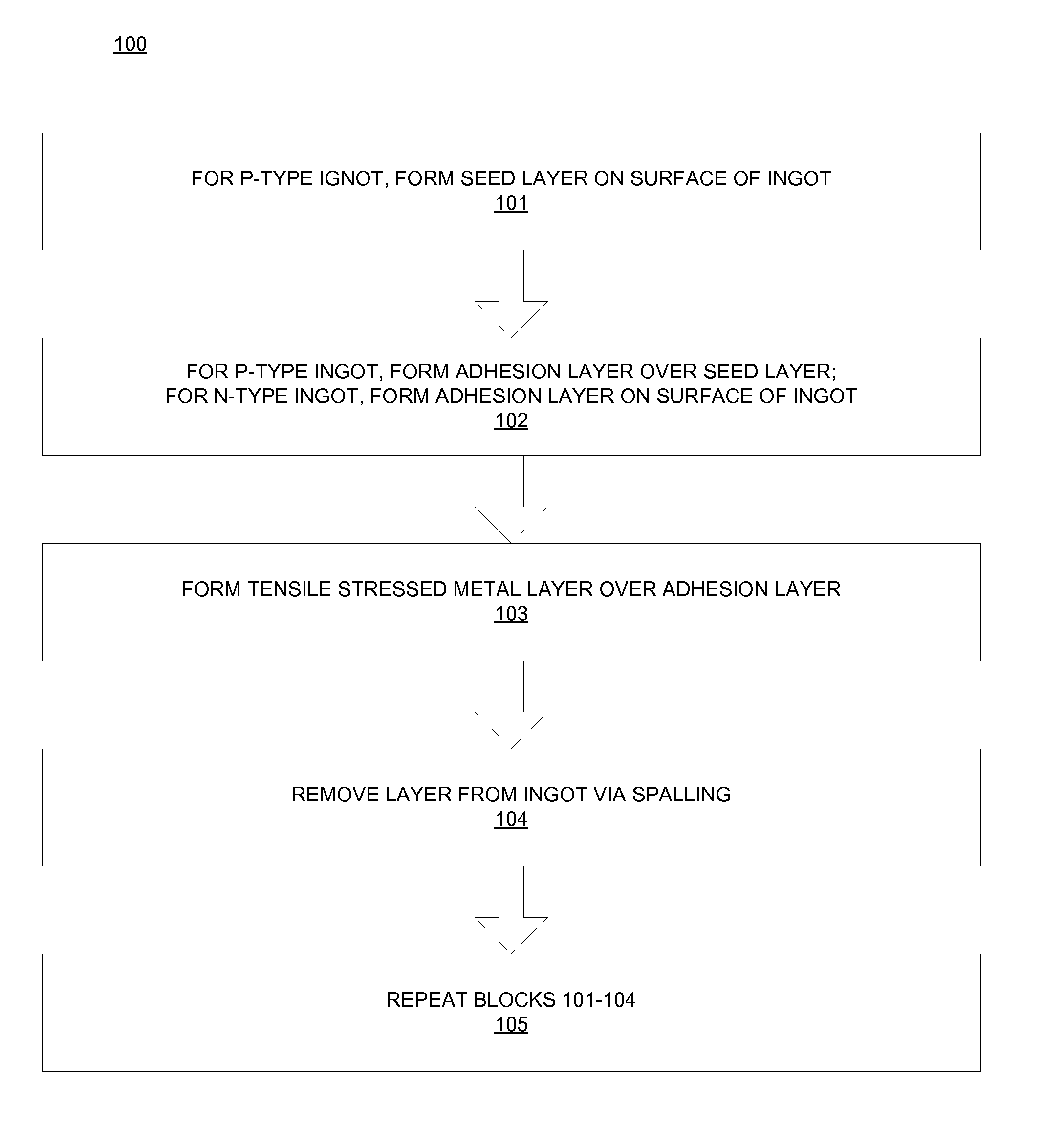
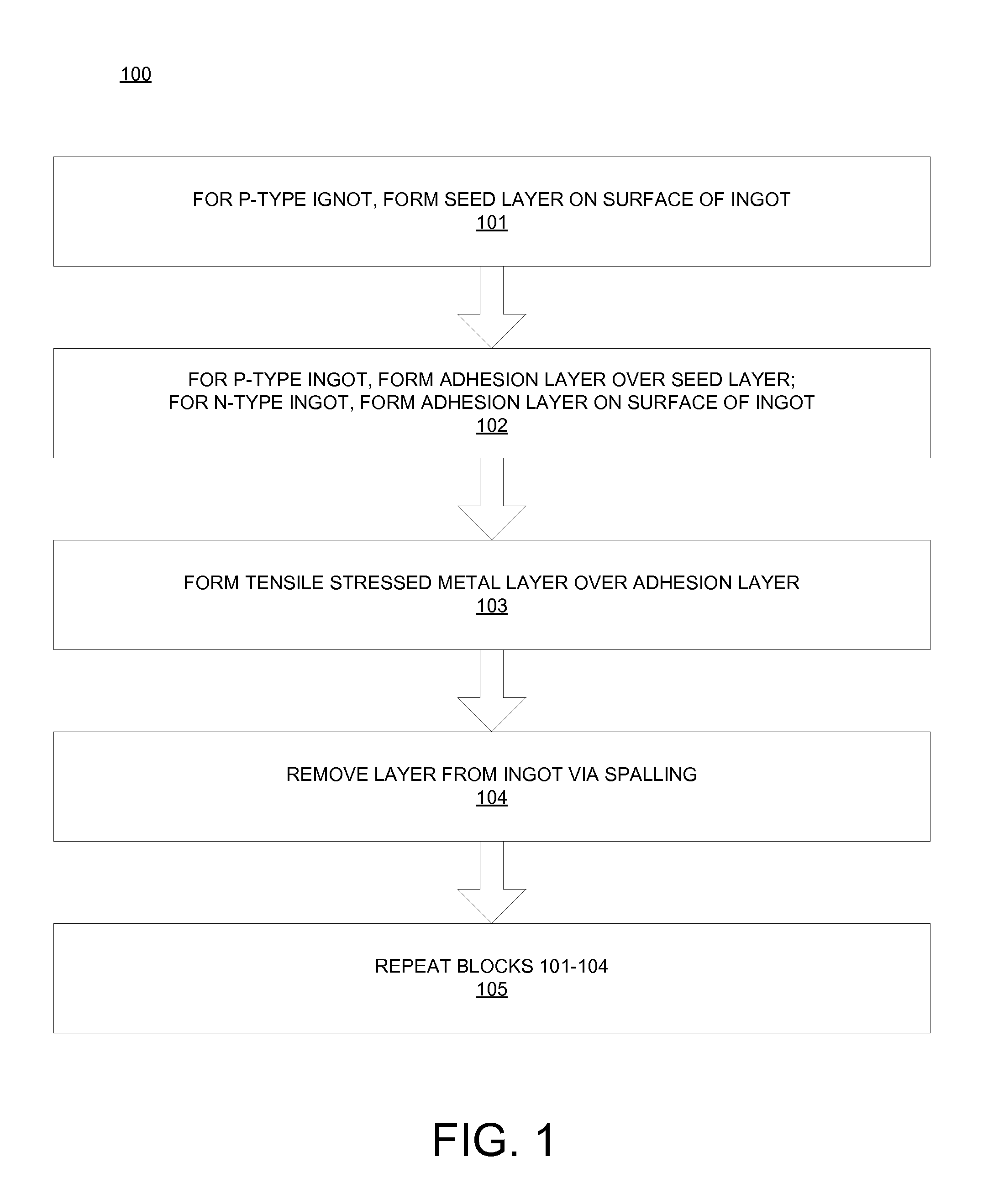
[0015]Embodiments of systems and methods for spalling for a semiconductor substrate are provided, with exemplary embodiments being discussed below in detail.

[0016]A layer of tensile stressed metal or metal alloy may be formed on a surface of an ingot of a semiconductor material to induce a fracture in the ingot by a process referred to as spalling. A layer of the semiconductor substrate having controlled thickness may be separated from the ingot at the fracture without kerf loss. The stressed metal layer may be formed by electroplating or electroless plating. Spalling may be used to cost-effectively form layers of semiconductor substrate for use in any semiconductor fabrication application, such as relatively thin semiconductor substrate wafers for photovoltaic (PV) cells, or relatively thick semiconductor-on-insulator for mixed-signal, radiofrequency (RF), or microelectromechanical (MEMS) applications.

[0017]FIG. 1 illustrates an embodiment of a method 100 for spalling for an ingot ...


PUM

PropertyMeasurementUnit
temperatureaaaaaaaaaa
thickaaaaaaaaaa
tensile stressaaaaaaaaaa

Abstract

A method for spalling a layer from an ingot of a semiconductor substrate includes forming a metal layer on the ingot of the semiconductor substrate, wherein a tensile stress in the metal layer is configured to cause a fracture in the ingot; and removing the layer from the ingot at the fracture. A system for spalling a layer from an ingot of a semiconductor substrate includes a metal layer formed on the ingot of the semiconductor substrate, wherein a tensile stress in the metal layer is configured to cause a fracture in the ingot, and wherein the layer is configured to be removed from the ingot at the fracture.

Description

CROSS-REFERENCE TO RELATED APPLICATION[0001]This application claims the benefit of U.S. Provisional Application No. 61 / 185,247, filed Jun. 9, 2009. This application is also related to attorney docket numbers YOR920100056US1, YOR920100058US1, YOR920100060US1, and FIS920100006US1, each assigned to International Business Machines Corporation (IBM) and filed on the same day as the instant application, all of which are herein incorporated by reference in their entirety.FIELD[0002]The present invention is directed to semiconductor substrate fabrication using stress-induced substrate spalling.DESCRIPTION OF RELATED ART[0003]A large portion of the cost of a semiconductor-based solar cell may be due to the cost of producing a layer of a semiconductor substrate on which to build the solar cell. In addition to the energy costs associated with the separation and purification of the substrate material, there is a significant cost associated with the growth of an ingot of the substrate material. ...

Claims


Application Information

Patent Timeline
Patent Type & Authority Applications(United States)
IPC IPC(8): B05D3/02
CPCH01L31/0725H01L31/074H01L31/075Y02E10/548H01L31/184H01L31/1892H01L31/076H01L21/02002Y02E10/546H01L21/02008H01L31/182
Inventor BEDELL, STEPHEN W.FOGEL, KEITH E.LAURO, PAUL A.SADANA, DEVENDRASHAHRJERDI, DAVOOD
Owner GLOBALFOUNDRIES INC
Why Eureka
Try Eureka