Method for assuring counterbore depth of vias on printed circuit boards and printed circuit boards made accordingly

a technology of printed circuit boards and counterbore depth, which is applied in the direction of high frequency circuit adaptation, inspection/indentification of circuits, instruments, etc., can solve the problems of increased signal degradation, particularly acute problem with respect to the use of vias, and the thick pcbs of the backplane on which such connector vias are commonly found, so as to achieve the effect of easy determination

Active Publication Date: 2010-12-16
CIENA
View PDF8 Cites 21 Cited by
  • Summary
  • Abstract
  • Description
  • Claims
  • Application Information

AI Technical Summary

Problems solved by technology

This problem is particularly acute with respect to vias used for connectors because such vias must have a certain close spacing (usually standardized) in order to properly mate with the connector pins of a plug-in card.
Also, the backplanes on which such connector vias are commonly found tend to be rather thick PCBs because they commonly must accommodate a large number of layers due to the need to route a large number of signals over the PCB.
On the other hand, if the drill does not drill far enough, then more copper will remain in the via than is necessary, leading to increased signal degradation.
However, there is no easy way to determine if the drill did not drill as deeply as desired (so that the signal degradation caused by the via is greater than it needs to be).
While there are ways to determine if the counterbore has not been drilled deep enough, they are not practical for standard PCB testing.
However, this is not a solution that can be reasonably implemented on a production scale because of the labor and cost involved.
However, this also is a time consuming and expensive proposition that is not reasonable to implement on a production scale.

Method used


Image

  • Method for assuring counterbore depth of vias on printed circuit boards and printed circuit boards made accordingly
  • Method for assuring counterbore depth of vias on printed circuit boards and printed circuit boards made accordingly
  • Method for assuring counterbore depth of vias on printed circuit boards and printed circuit boards made accordingly

Examples


Embodiment Construction

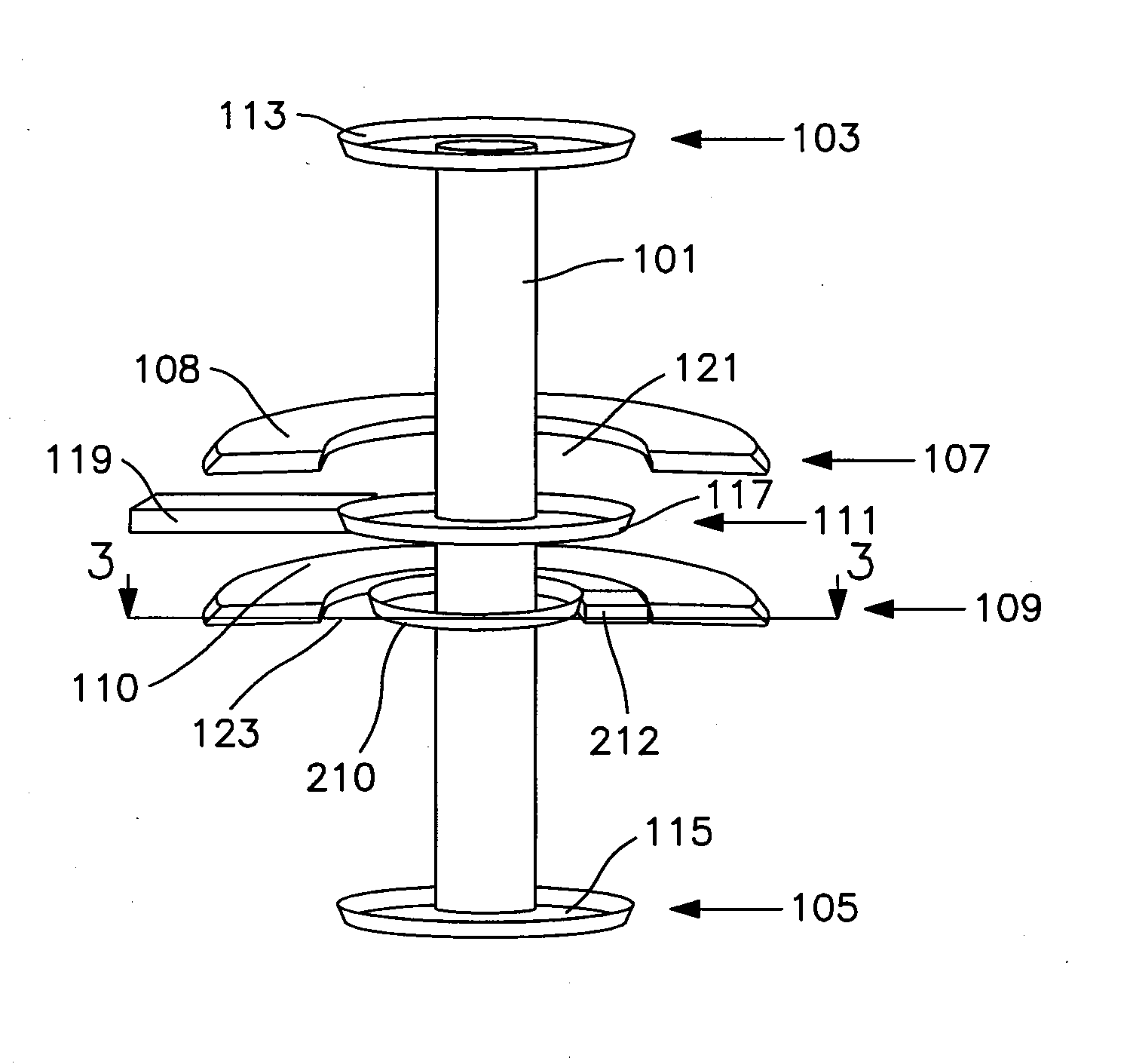
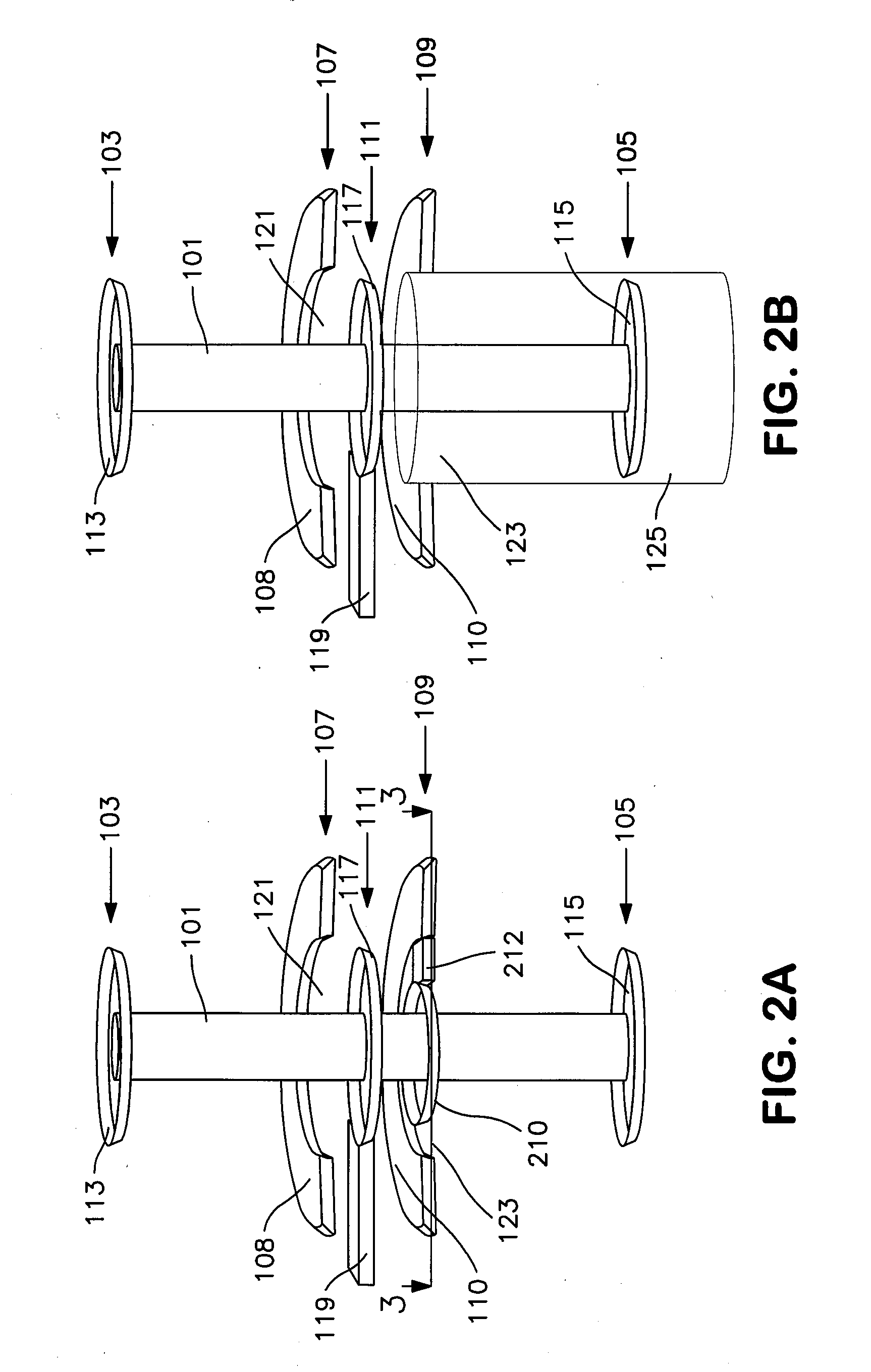
[0021]FIGS. 2A and 2B are elevation views before and after counterboring, respectively, of a via similar to the one shown in FIGS. 1A and 1B, but modified in accordance with the principles of a first embodiment of the present invention. Most of the features shown in FIGS. 2A and 2B are the same as features shown in FIGS. 1A and 1B. Hence, like components have been labeled with the same reference numerals in FIGS. 2A and 2B as in FIGS. 1A and 1B.

[0022]With reference to FIG. 2A, the top layer 103, the bottom layer 105, the upper ground plane layer 107, and the signal layer 111 are essentially unchanged from FIGS. 1A and 1B. However, the lower ground plane layer 109 differs in that, in the middle of the anti-pad 123, a conductive pad 210 has been added surrounding the via (similar in nature to pad 117 in the signal layer 111. This pad makes contact with the copper in the via 101. Furthermore, a signal path 212 has been added that runs the short distance through the anti-pad area 123 be...


PUM

PropertyMeasurementUnit
frequencyaaaaaaaaaa
impedanceaaaaaaaaaa
impedanceaaaaaaaaaa

Abstract

A method is disclosed for fabricating a PCB so that is can easily be determined if a via in the PCB has not been counterbored to a desired depth. A PCB fabricated according to the method also is disclosed.

Description

FIELD OF THE INVENTION [0001]The invention pertains to printed circuit board (PCB) fabrication. More particularly, the invention pertains to counter boring of vias on printed circuit boards.BACKGROUND OF THE INVENTION [0002]Printed circuit boards are used in many electronic devices for purposes of routing signals between electrical and electronic components that are (1) mounted on the PCB, (2) connected to the PCB via edge connectors, or (3) fabricated directly into the PCB. PCBs generally are flat square or rectangular boards primarily formed of a dielectric material with copper or other conductive traces formed therein to route signals between the various aforementioned electronic components. The term circuitry shall be used herein to refer broadly to any form of electrical or electronic components, including analog components, digital components, ground planes, and simple conductors such as copper traces.[0003]A PCB has two opposing external major surfaces, one or both of which m...

Claims


Application Information

Patent Timeline
Patent Type & Authority Applications(United States)
IPC IPC(8): H05K1/11G01R19/00G01R31/02H01R43/00
CPCG01R31/024H05K1/0245H05K1/0251H05K1/0268H05K1/116H05K3/0047H05K3/429H05K2201/09454H05K2201/09627H05K2201/09636H05K2201/09718H05K2201/09781H05K2203/0207H05K2203/0242H05K2203/175Y10T29/49117G01R31/2818G01R31/2805G01R31/2812
Inventor TWARDY, CRAIGMCDONALD, ROBERT
Owner CIENA
Why Eureka
Try Eureka