Composition for forming base film for lithography and method for forming multilayer resist pattern
a technology of lithography and base film, applied in the direction of optics, basic electric elements, electric apparatus, etc., can solve the problems of difficult to increase the aspect ratio, difficult to etch, and variable problems, and achieve excellent etching resistance and excellent resist pattern
- Summary
- Abstract
- Description
- Claims
- Application Information
AI Technical Summary
Benefits of technology
Problems solved by technology
Method used
Image
Examples
example
[0157]The present invention will be specifically described with reference to synthesis examples, examples and comparative examples below, but the present invention is not limited to the description. The molecular weight was measured specifically in the following manner. A weight average molecular weight (Mw) and a number average molecular weight (Mn) of polystyrene conversion were measured by gel permeation chromatography (GPC), and a dispersion degree (Mw / Mn) was obtained. A weight reduction rate upon increasing the temperature from 40° C. to 400° C. at 10° C. per minute was measured with a calorimeter (TGA).
(1) Synthesis Example of DMN Resin (1,5-DMN-R)
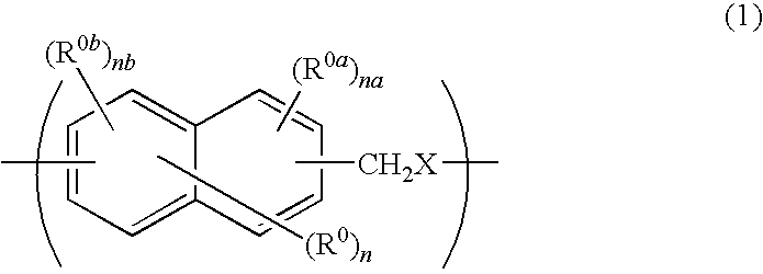
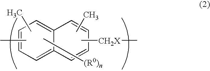
[0158]1,5-Dimethylnaphthalene (1,5-DMN), produced by Mitsubishi Gas Chemical Co., Inc., (218 g, 1.4 mol), a 40% formalin aqueous solution, produced by Mitsubishi Gas Chemical Co., Inc., (420 g, 5.6 mol) and 98% sulfuric acid, produced by Kanto Kagaku Co., Ltd., (194 g) were charged under a nitrogen stream into a four-neck flask (2 L...
example 22
[0185]The solution of the material for forming an underlayer film (Example 6) was coated on an SiO2 substrate having a thickness of 300 nm and baked at 300° C. for 120 seconds to form an underlayer film having a thickness of 80 nm. An ArF resist solution was coated thereon and baked at 130° C. for 60 seconds to form a photoresist layer having a thickness of 150 nm. The ArF resist solution was prepared by mixing 5 parts of the compound represented by the following formula (110), 1 part of triphenylsulfonium nonafluoromethanesulfonate, 2 parts of tributylamine and 92 parts of PGMEA.
[0186]Subsequently, the assembly was exposed with an electron beam patterning device (ELS-7500, produced by Elionix Co., Ltd., 50 keV), baked at 115° C. for 90 seconds (PEB), and developed with a 2.83% by mass tetramethylammonium hydroxide (TMAH) aqueous solution for 60 seconds, thereby providing a positive pattern. The results of observation of the resulting pattern of 60 nm L / S (1 / 1) are shown in Table 2....
PUM
| Property | Measurement | Unit |
|---|---|---|
| refractive index | aaaaa | aaaaa |
| boiling point | aaaaa | aaaaa |
| temperature | aaaaa | aaaaa |
Abstract
Description
Claims
Application Information


