
Method of detecting an attack by fault injection on a memory device, and corresponding memory device

Active Publication Date: 2010-12-16
STMICROELECTRONICS SRL
View PDF18 Cites 12 Cited by
  • Summary
  • Abstract
  • Description
  • Claims
  • Application Information

AI Technical Summary

Benefits of technology

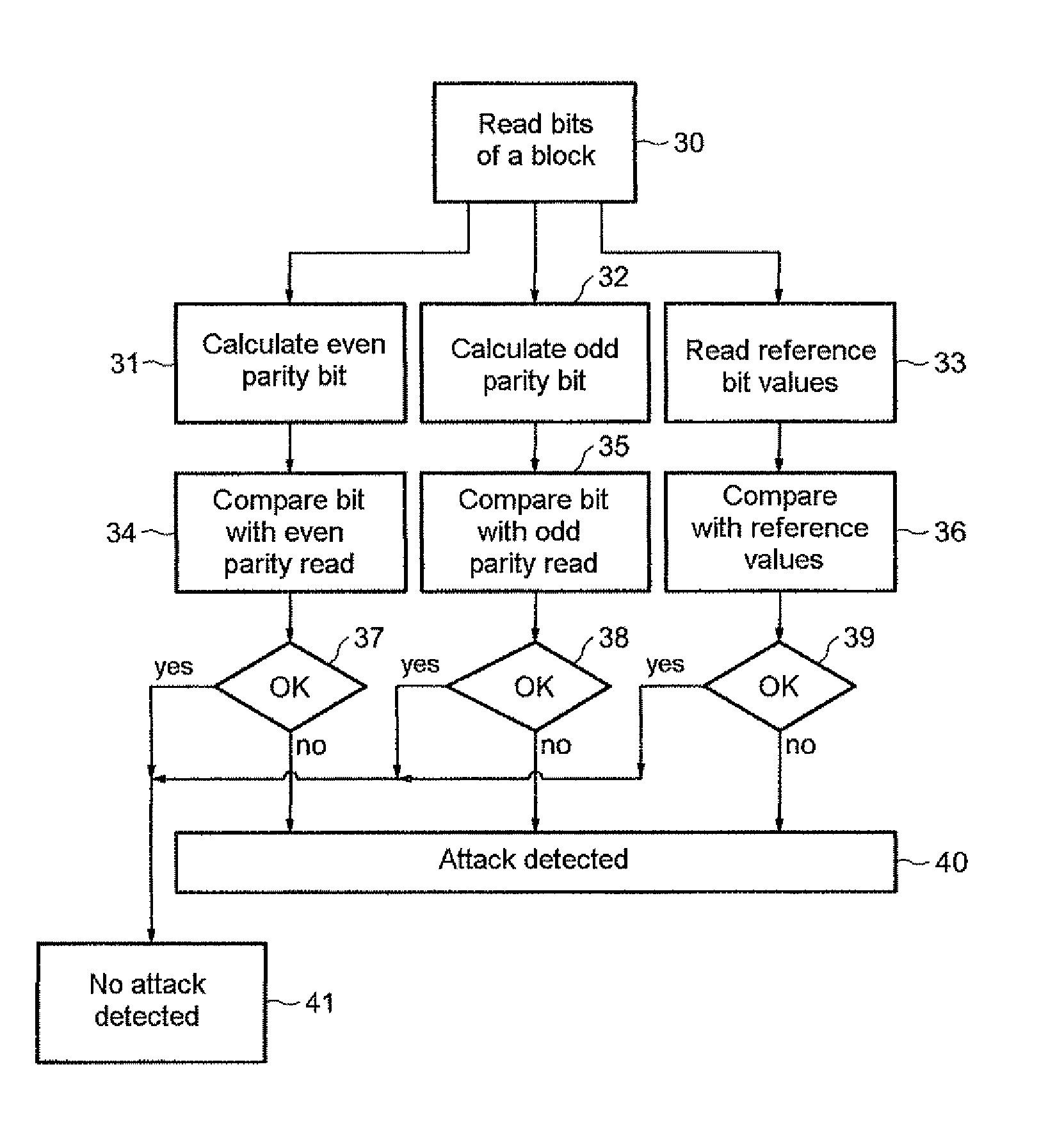
[0005]According to a first implementation and embodiment, a method of detecting an attack by fault injection on a memory device and a corresponding memory device are proposed, offering a more reliable detection of an attack by fault injection. According to one aspect, a method of detecting an attack by fault injection on a memory device including at least one group of memory cells configured to store at least one block of bits comprising data bits and m parity bits is proposed. The detection may include, when reading a block, a read of each bit of the block included in the corresponding memory cell and a parity check performed on the basis of the read value of each data bit and the read value of each parity bit.
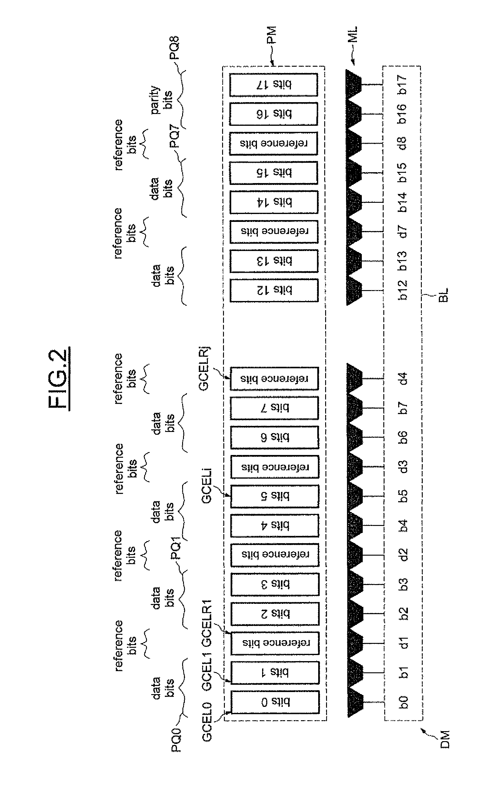
[0007]Thus, for example, inserting reference bits at selected points of the memory plane, and storing between these reference bits of the block that have to be read associated with different parities, may make it possible to detect an attack by fault injection, even when a laser beam is sufficiently wide to illuminate two memory cells likely to include two bits of the same parity. This is because, in this case, the laser beam may also affect a reference bit by toggling its value, which may provoke an attack detection signal. Moreover, a bit associated with a given parity can be either a data bit having the parity, or even the parity bit itself relating to that parity. Although a number of placements are possible for the insertion of the reference memory cells, in particular the correspondence between the ranks of the bits and the memory cells intended to store these bits, it may be particularly advantageous to provide for insertion of a reference memory cell every m memory cells.

Problems solved by technology

This is because, in this case, the laser beam may also affect a reference bit by toggling its value, which may provoke an attack detection signal.

Method used


Image

  • Method of detecting an attack by fault injection on a memory device, and corresponding memory device
  • Method of detecting an attack by fault injection on a memory device, and corresponding memory device
  • Method of detecting an attack by fault injection on a memory device, and corresponding memory device

Examples


Embodiment Construction

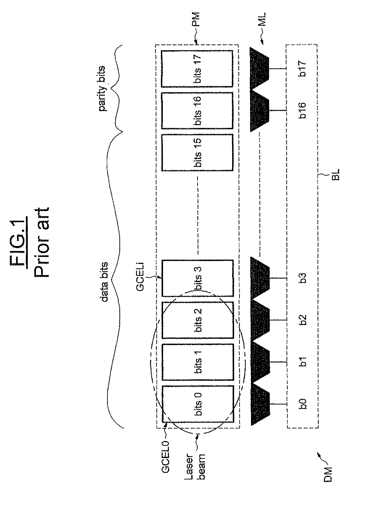
[0020]In FIG. 1, the reference DM designates a conventional memory device whose memory plane PM includes sets of memory cells GCELi. The memory cells of one and the same set are configured to store the bits of the same rank of the different blocks of bits BL that have to be stored in the memory plane. More specifically, in the example described here, a block of bits BL that has to be stored in the memory plane includes data bits, in this case 16 (ranked 0 to 15), and parity bits, in this case two, ranked 16 and 17.

[0021]Also, for a given block BL, the memory cell CEL0 is configured to store the bit b0 of rank 0. The memory cell CEL1 is configured to store the bit b1 of rank 1 and, more generally, the memory cell CELi is configured to store the bit bi of rank i. The group of memory cells CELi is therefore configured to store the block BL.

[0022]The memory device has a bit-by-bit architecture, which means that, when a block BL is read, all the bits of the block can be read individually...


PUM


Abstract

A memory device may include a memory plane including a group of memory cells configured to store a block of bits including data bits and parity bits, and a detector for detecting a fault injection including a reader to read each bit, and a first checker to perform, when reading a block, a parity check based on the read value of each data and parity bit. The memory plane may include reference memory cells arranged between some of the memory cells to create packets of m memory cells. Each reference memory cell may store a reference bit and each packet of m memory cells may store m bits of the associated block, when m is greater than 1, with different parities. The detector may further include a second checker to perform, when reading the block, a check on the value of each reference bit.

Description

FIELD OF THE INVENTION[0001]The invention relates, generally, to electronic circuits, and more particularly to the detection of an attack by fault injection on a memory device. The invention applies advantageously but in a nonlimiting way to chip cards and to the protection of the confidential data that they contain.BACKGROUND OF THE INVENTION[0002]Among the possible attacks made by hackers to extract confidential data from a memory, for example, protected memory of a chip card, there are the attacks by fault injection (DFA or “Differential Fault Analysis”) that aim to disrupt the operation and / or the content of the memory, for example, by means of radiation (laser, infrared, X-rays, etc.).[0003]It therefore may be particularly useful to be able to detect such an attack by fault injection. Once the attack is detected, there may be many approaches depending on the application for either blocking the component, preventing the sensitive data from being handed over, or reinitializing th...

Claims


Application Information

Patent Timeline
IPC IPC(8): H03M13/09G06F11/10
CPCG11C7/24G06F11/1032
Inventor LISART, MATHIEUMERCIER, JULIEN
Owner STMICROELECTRONICS SRL
Learn More