Avalanche Photodiode

a photodiode and avalanche technology, applied in the field of photodetection, can solve the problems that conventional apds are often not suitable for “back-side” illuminated devices, and achieve the effect of higher signal-to-noise ratio

Inactive Publication Date: 2010-12-30
RAYTHEON CO
View PDF2 Cites 61 Cited by
  • Summary
  • Abstract
  • Description
  • Claims
  • Application Information

AI Technical Summary

Benefits of technology

The invention provides a photodiode that has better quality signals than older versions.

Problems solved by technology

The technical problem addressed by this patent is finding alternative types of photosensors that can detect small amounts of light without amplifying background signals or being negatively affected by back-side illumination.

Method used


Image

  • Avalanche Photodiode
  • Avalanche Photodiode
  • Avalanche Photodiode

Examples


Embodiment Construction

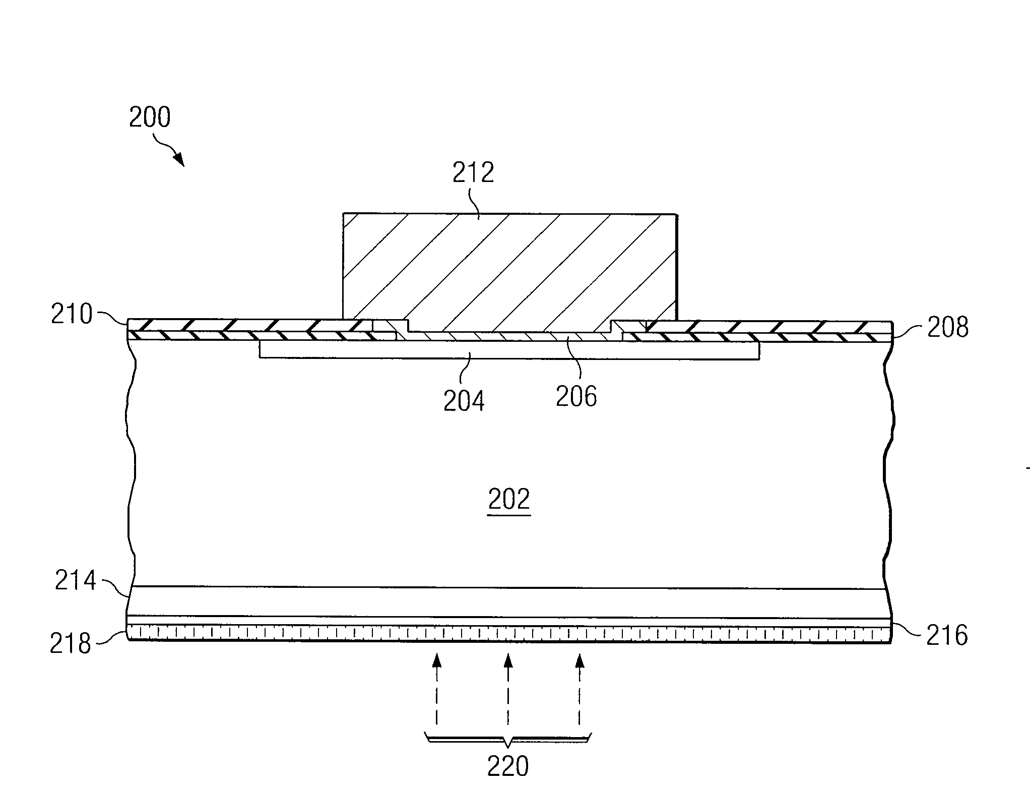
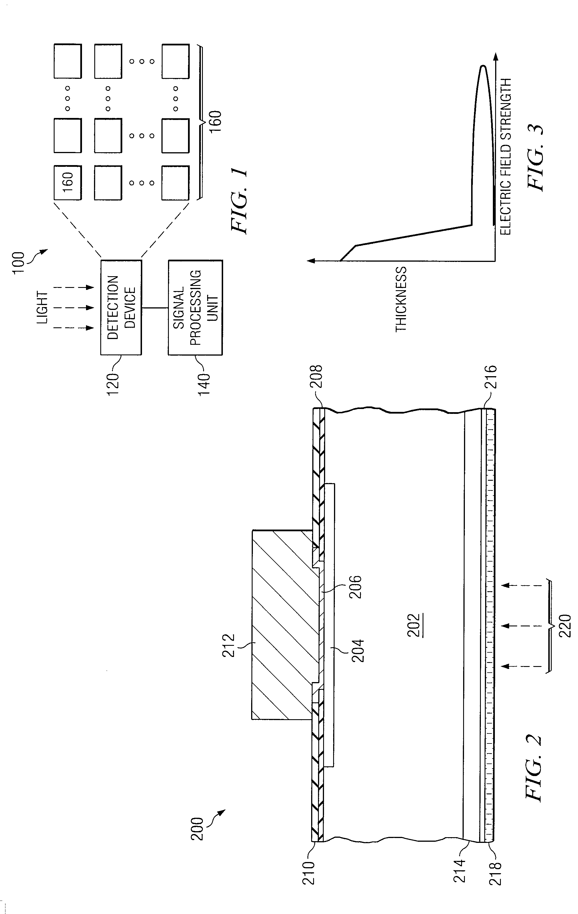
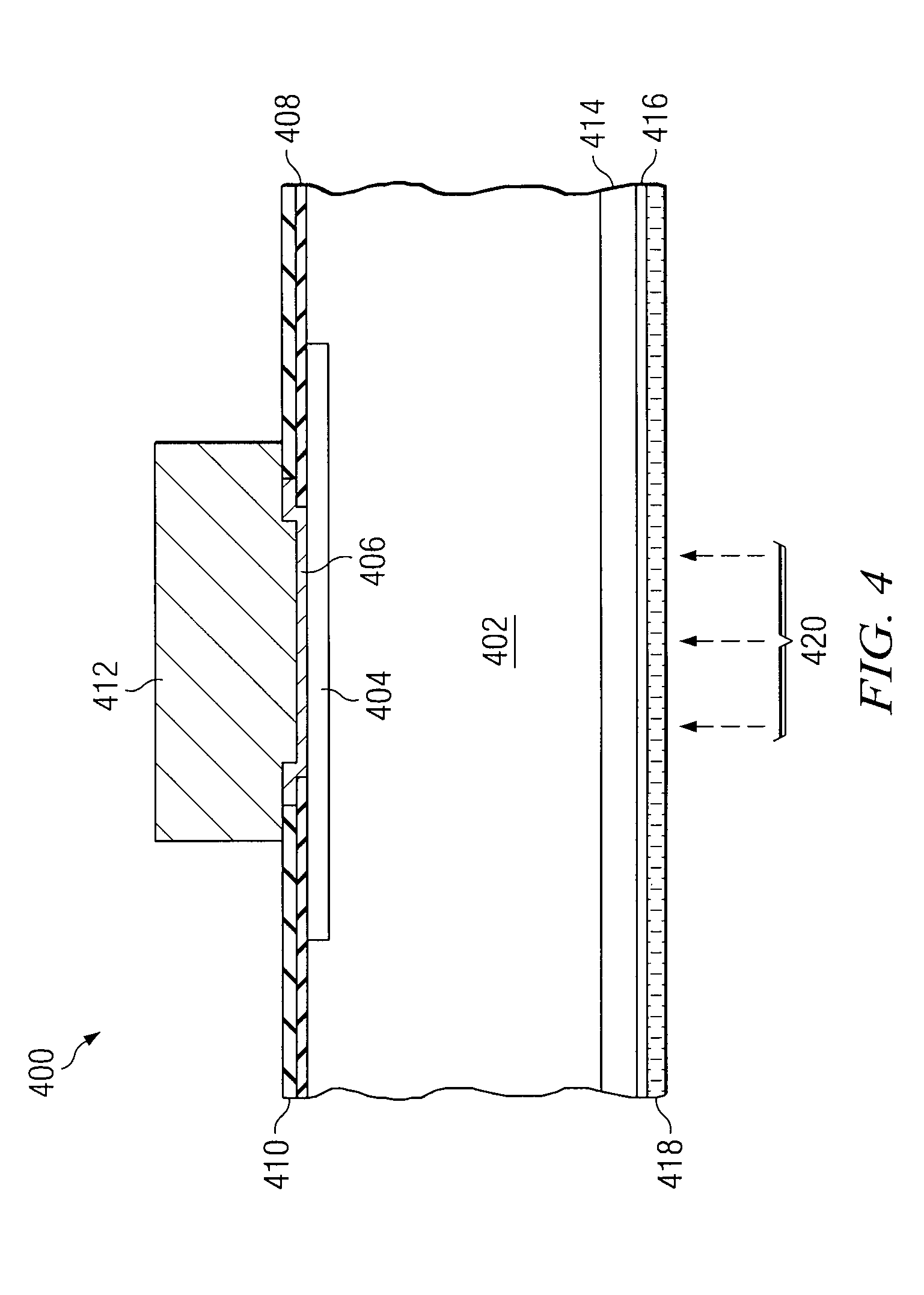
[0012]Embodiments of the present disclosure and its advantages are best understood by referring to FIGS. 1 through 4 of the drawings, like numerals being used for like and corresponding parts of the various drawings.

[0013]FIG. 1 is a block diagram illustrating photodetection system 100, in accordance with embodiments of the present disclosure. For example, photodetection system 100 may be a digital camera, video camera, or any other photographic device, image capturing device, and / or high-speed photon counting device. Photodetection system 100 may include detection device 120 and signal processing unit 140. Detection device 120 may be a focal plane array (FPA), active pixel sensor (APS) or any other suitable light sensing device that can capture photons. Detection device 120 may include, for example, one or more diodes, complimentary metal-oxide semiconductors (CMOSs), charge-coupled devices (CCDs), or any other suitable photovoltaic detectors or transducers. Signal processing unit ...


PUM


Abstract

A photodiode may include a first region comprising substantially intrinsic semiconductor material, the region having a first side and a second side opposite to the first side. The photodiode may also include a second region comprising highly-doped p-type semiconductor material formed proximate to the first side of the first region. The photodiode may additionally include a third region comprising highly-doped n-type semiconductor material formed proximate to the second side of the first region. The photodiode may further include a fourth region comprising one of: (i) highly-doped p-type semiconductor formed between the first region and the third region, or (ii) highly-doped n-type semiconductor formed between the first region and the second region.

Description


Claims


Application Information

Patent Timeline
Owner RAYTHEON CO
Why Eureka
Try Eureka