Formation of TSV Backside Interconnects by Modifying Carrier Wafers

a backside and interconnect technology, applied in the field of integrated circuit structures, can solve the problems of reducing the size of the component, the minimum size needed to make these components, and the density that can be achieved in two dimensions, so as to improve the ability to secure the carrier wafer, reduce particle generation, and ensure the effect of alignmen

Active Publication Date: 2010-12-30
TAIWAN SEMICON MFG CO LTD
View PDF60 Cites 55 Cited by
  • Summary
  • Abstract
  • Description
  • Claims
  • Application Information

AI Technical Summary

Benefits of technology

[0012]The advantageous features of the present invention include more reliable alignment, reduced particle generation, and improved ability for securing carrier wafers on E-chucks.

Problems solved by technology

Although dramatic improvements in lithography have resulted in considerable improvements in 2D integrated circuit formation, there are physical limitations to the density that can be achieved in two dimensions.
One of these limitations is the minimum size needed to make these components.
Also, when more devices are put into one chip, more complex designs are required.
An additional limitation comes from the significant increase in the number and lengths of interconnections between devices as the number of devices increases.
When the number and the lengths of interconnections increase, both circuit RC delay and power consumption increase.
The conventional formation process of backside TSV connections suffers from drawbacks.
Another problem is the difficulty in finding notches. FIG. 2A illustrates a top view of the structure shown in FIG. 1.
Since UBM 108 is not transparent, instruments such as photo steppers often cannot find notch 112, and hence cannot perform alignments for the subsequent processes.
However, carrier wafer 104 is typically formed of glass and cannot be secured on the ESC firmly.
This is partially due to the inadequate mobile ions in the glass.

Method used


Image

  • Formation of TSV Backside Interconnects by Modifying Carrier Wafers
  • Formation of TSV Backside Interconnects by Modifying Carrier Wafers
  • Formation of TSV Backside Interconnects by Modifying Carrier Wafers

Examples


Embodiment Construction

[0018]The making and using of the embodiments of the present invention are discussed in detail below. It should be appreciated, however, that the embodiments provide many applicable inventive concepts that can be embodied in a wide variety of specific contexts. The specific embodiments discussed are merely illustrative of specific ways to make and use the invention, and do not limit the scope of the invention.

[0019]A method for forming a novel backside interconnect structure connecting to through-silicon vias (TSVs, also known as through-semiconductor vias) is provided. The intermediate stages in the manufacturing of an embodiment are illustrated. The variations of the embodiments are discussed. Throughout the various views and illustrative embodiments, like reference numbers are used to designate like elements.

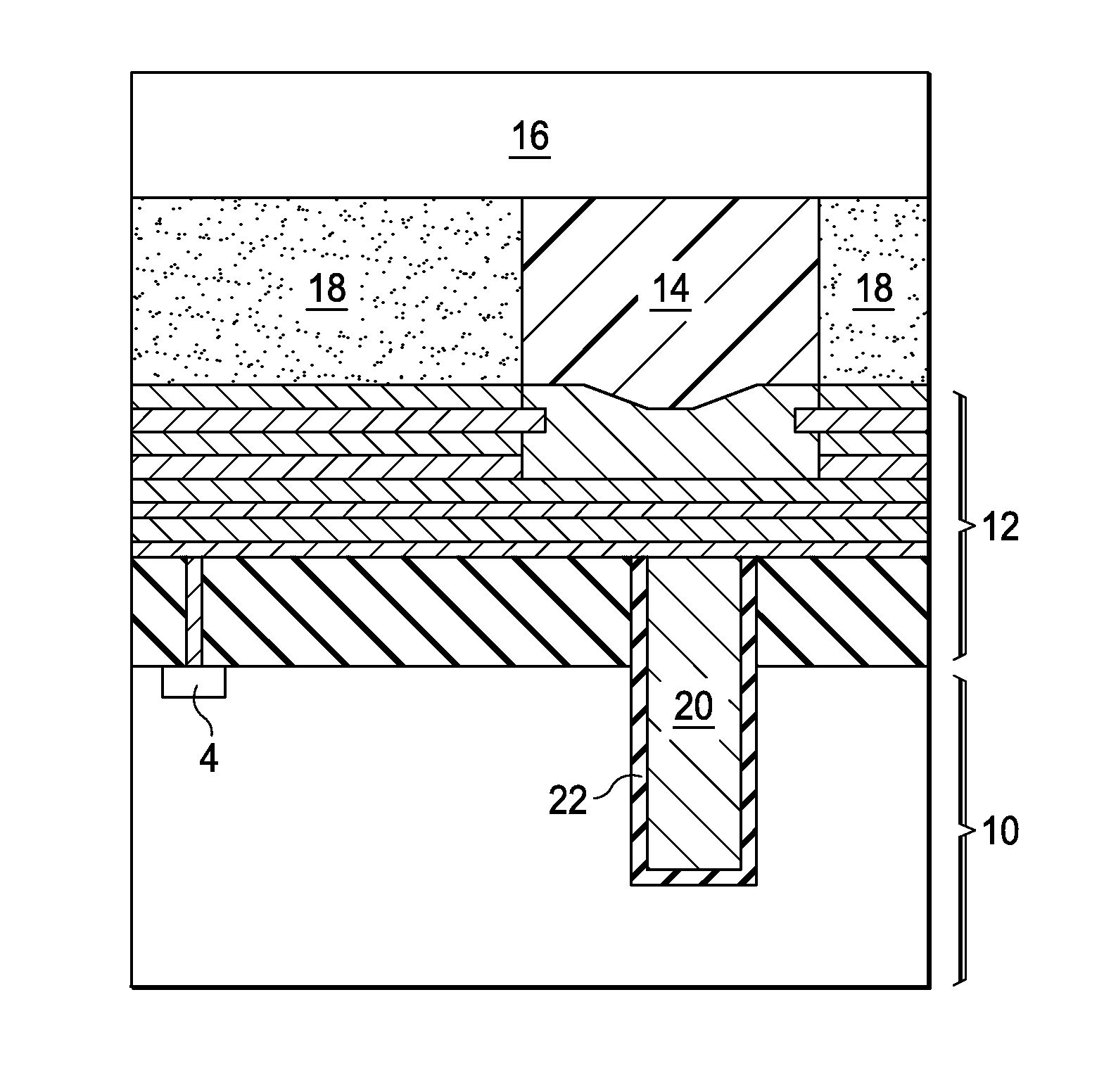
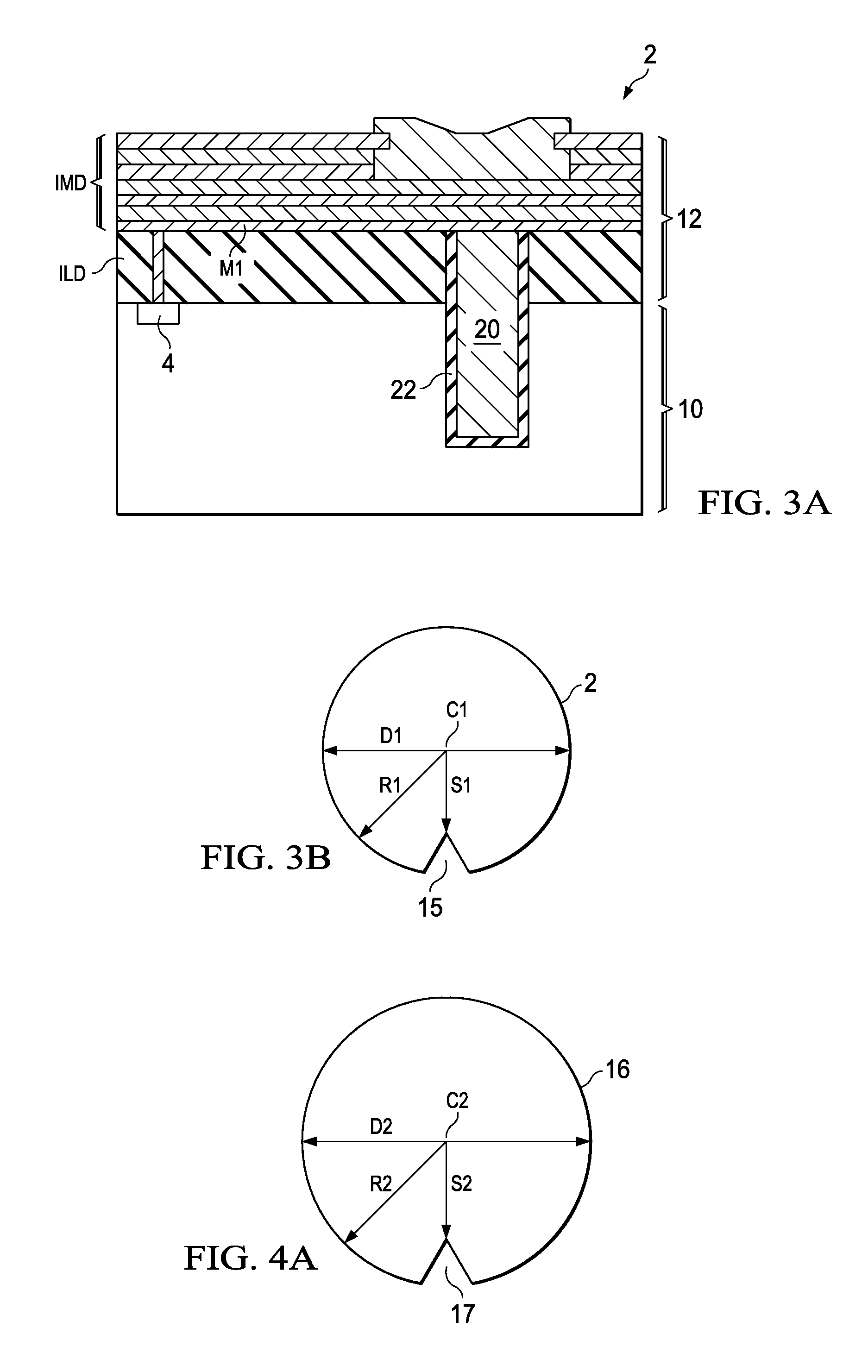
[0020]Referring to FIG. 3A, wafer 2, which includes substrate 10, is provided. Substrate 10 may be a semiconductor substrate, such as a bulk silicon substrate, although it ma...


PUM


Abstract

An integrated circuit structure includes a semiconductor wafer, which includes a first notch extending from an edge of the semiconductor wafer into the semiconductor wafer. A carrier wafer is mounted onto the semiconductor wafer. The carrier wafer has a second notch overlapping at least a portion of the first notch. A side of the carrier wafer facing the semiconductor wafer forms a sharp angle with an edge of the carrier wafer. The carrier wafer has a resistivity lower than about 1×10⁸ Ohm-cm.

Description

[0001]This application claims the benefit of U.S. Provisional Application No. 61 / 220,803 filed on Jun. 26, 2009, entitled “Improving the Formation of TSV Backside Interconnects by Modifying Carrier Wafers,” which application is hereby incorporated herein by reference.TECHNICAL FIELD[0002]This invention relates generally to integrated circuit structures, and more particularly to through-silicon vias, and even more particularly to the formation of interconnect structures on the backside of wafers and connected to the through-silicon vias.BACKGROUND[0003]Since the invention of integrated circuits, the semiconductor industry has experienced continuous rapid growth due to constant improvements in the integration density of various electronic components (i.e., transistors, diodes, resistors, capacitors, etc.). For the most part, this improvement in integration density has come from repeated reductions in minimum feature size, allowing more components to be integrated into a given chip are...

Claims


Application Information

Patent Timeline
Patent Type & Authority Applications(United States)
IPC IPC(8): H01L21/768H01L21/77
CPCH01L21/6836H01L23/481H01L23/544H01L24/11H01L24/13H01L24/14H01L24/16H01L24/81H01L25/0657H01L2221/6834H01L2221/68372H01L2223/54453H01L2223/54493H01L2224/11002H01L2224/1147H01L2224/11901H01L2224/1308H01L2224/13082H01L2224/13083H01L2224/131H01L2224/13124H01L2224/13139H01L2224/13144H01L2224/13147H01L2224/13155H01L2224/13184H01L2224/81193H01L2224/81801H01L2225/06513H01L2225/06541H01L2924/01011H01L2924/01012H01L2924/01013H01L2924/0102H01L2924/01029H01L2924/01047H01L2924/01078H01L2924/01079H01L2924/01082H01L2924/09701H01L2924/14H01L2924/19041H01L2924/19043H01L2924/3511H01L2924/00013H01L2924/01006H01L2924/01019H01L2924/01023H01L2924/01033H01L2924/01074H01L2924/01075H01L2924/014H01L2924/01327H01L2924/00014H01L2224/13099H01L24/03H01L24/05H01L2224/0231H01L2224/02351H01L2224/02372H01L2224/05001H01L2224/05008H01L2224/05009H01L2224/05024H01L2224/05025H01L2224/05026H01L2224/05124H01L2224/05139H01L2224/05144H01L2224/05147H01L2224/05184H01L2224/05548H01L2224/0557H01L2224/05571H01L2224/05624H01L2224/05639H01L2224/05644H01L2224/05647H01L2224/05655H01L2224/13007H01L2224/13024H01L2924/013
Inventor HUANG, HON-LINHSIAO, CHING-WENHSU, KUO-CHINGCHEN, CHEN-SHIEN
Owner TAIWAN SEMICON MFG CO LTD
Why Eureka
Try Eureka