Color filter array on pixel array substrate and display panel

a color filter array and substrate technology, applied in non-linear optics, instruments, optics, etc., can solve the problems of reducing the contrast the misalignment of the lcd panel, etc., to improve the alignment accuracy, reduce the fabrication cost, and improve the production yield

Active Publication Date: 2011-01-06
AU OPTRONICS CORP
View PDF12 Cites 30 Cited by
  • Summary
  • Abstract
  • Description
  • Claims
  • Application Information

AI Technical Summary

Benefits of technology

[0008]The present invention is directed to a color filter array on pixel array substrate, which can improve an alignment accuracy during a fabrication process thereof, so as to improve a production yield and reduce a fabrication cost.

Problems solved by technology

However, such LCD panel may have a misalignment problem when the color filter substrate and the TFT array substrate are assembled.
However, when the black matrix material layer with a slight light transmittance is used for the above benefit, after the black matrix is patterned, it probably cannot achieve a total light-shielding effect, which may lead to a decrease of a contrast of the LCD panel, and a display quality thereof is influenced.

Method used


Image

  • Color filter array on pixel array substrate and display panel
  • Color filter array on pixel array substrate and display panel
  • Color filter array on pixel array substrate and display panel

Examples


Embodiment Construction

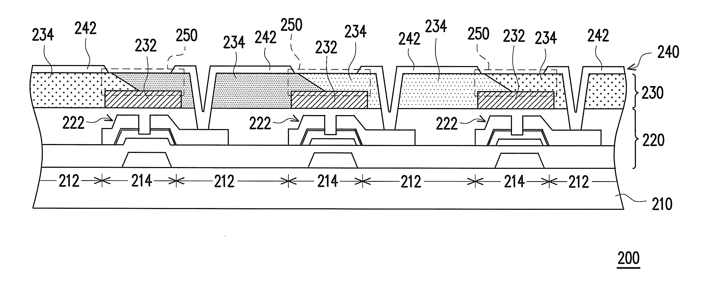
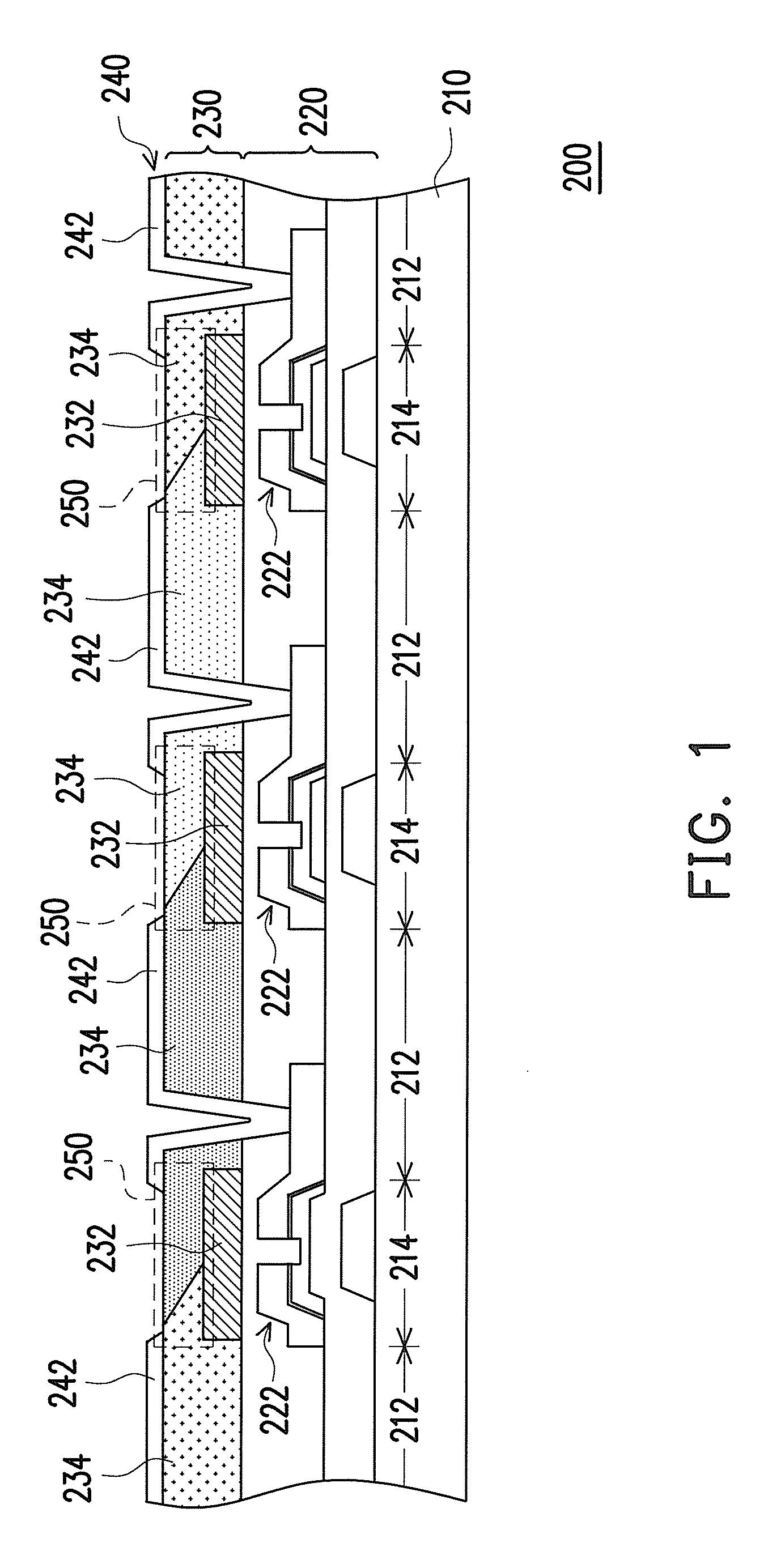
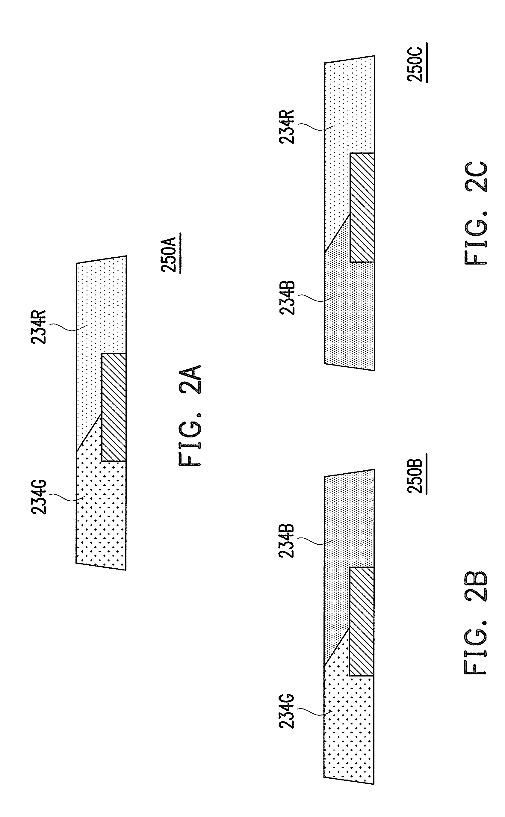
[0023]FIG. 1 is a partial cross-sectional view of a color filter array on pixel array substrate according to an embodiment of the present invention. Referring to FIG. 1, the color filter array on pixel array substrate 200 of the present invention includes a substrate 210, an active device array 220, a color filter array 230 and a pixel electrode layer 240. In detail, the substrate 210 has a plurality of pixel regions 212 and a light-shielding region 214. Particularly, the light-shielding region 214 surrounds each of the pixel regions 212. The active device array 220 is disposed on the substrate 210. The color filter array 230 is disposed on the substrate 210, and includes a light-shielding patterned layer 232 located at the light-shielding region 214 and a plurality of color filter patterns 234. The color filter patterns 234 are respectively disposed in the pixel regions 212 and extend from the pixel regions 212 to the light-shielding region 214, wherein the color filter patterns 23...


PUM

PropertyMeasurementUnit
thicknessaaaaaaaaaa
optical densityaaaaaaaaaa
sizeaaaaaaaaaa

Abstract

A color filter array on pixel array substrate including a substrate, an active device array, a color filter array and a pixel electrode layer is provided. The substrate has a plurality of pixel regions and a light-shielding region. The active device array is disposed on the substrate. The color filter array is disposed on the substrate, and includes a light shielding patterned layer and a plurality of color filter patterns, wherein the light-shielding patterned layer is disposed in the light-shielding region. The color filter patterns are respectively disposed in the pixel regions and extend from the pixel regions into the light shielding regions, wherein the color filter patterns extending from adjacent pixel regions constitute a stacked structure within the light shielding regions. The pixel electrode layer is electrically connected to the active device array.

Description

CROSS-REFERENCE TO RELATED APPLICATION[0001]This application claims the priority benefit of Taiwan application serial no. 98122772, filed Jul. 6, 2009. The entirety of the above-mentioned patent application is hereby incorporated by reference herein and made a part of specification.BACKGROUND OF THE INVENTION[0002]1. Field of the Invention[0003]The present invention relates to a substrate and a display panel. More particularly, the present invention relates to a color filter array on pixel array substrate, and a display panel.[0004]2. Description of Related Art[0005]Since a liquid crystal display (LCD) has advantages of high display quality, small size, light weight, low driving voltage, low power consumption and wide application range, etc, it has replaced a cathode ray tube (CRT) and become a main stream in the display market. A conventional LCD panel is composed of a color filter substrate, a thin film transistor (TFT) array substrate and a liquid crystal layer disposed between t...

Claims


Application Information

Patent Timeline
Patent Type & Authority Applications(United States)
IPC IPC(8): G02F1/1335
CPCG02F2001/136222G02F1/136209G02F1/136222
Inventor TSENG, CHIN-ANHOU, HUNG-LUNGLEE, CHIA-YUHUANG, YEN-HENGCHEN, CHUNG-KAICHEN, CHIEH-WEILIN, YI-TSUN
Owner AU OPTRONICS CORP
Why Eureka
Try Eureka