Semiconductor memory device

a memory device and semiconductor technology, applied in semiconductor devices, capacitors, electrical devices, etc., can solve the problems of increasing manufacturing costs, becoming more difficult to form holes having a desired shape by dry etching, etc., and achieve the effect of large electrostatic capacitance and low cos

Inactive Publication Date: 2011-01-20
ELPIDA MEMORY INC
View PDF2 Cites 7 Cited by
  • Summary
  • Abstract
  • Description
  • Claims
  • Application Information

AI Technical Summary

Benefits of technology

[0026]According to an embodiment, it is possible to provide a highly-integrated semiconductor memory device including a capacitor having large electrostatic capacitance and capable of being manufactured at low costs.

Problems solved by technology

With an increase in the aspect ratio, however, it becomes more difficult to form a hole having a desired shape by dry etching.
Thus, the technique has the problem of an increase in manufacturing costs.

Method used


Image

  • Semiconductor memory device
  • Semiconductor memory device
  • Semiconductor memory device

Examples


Embodiment Construction

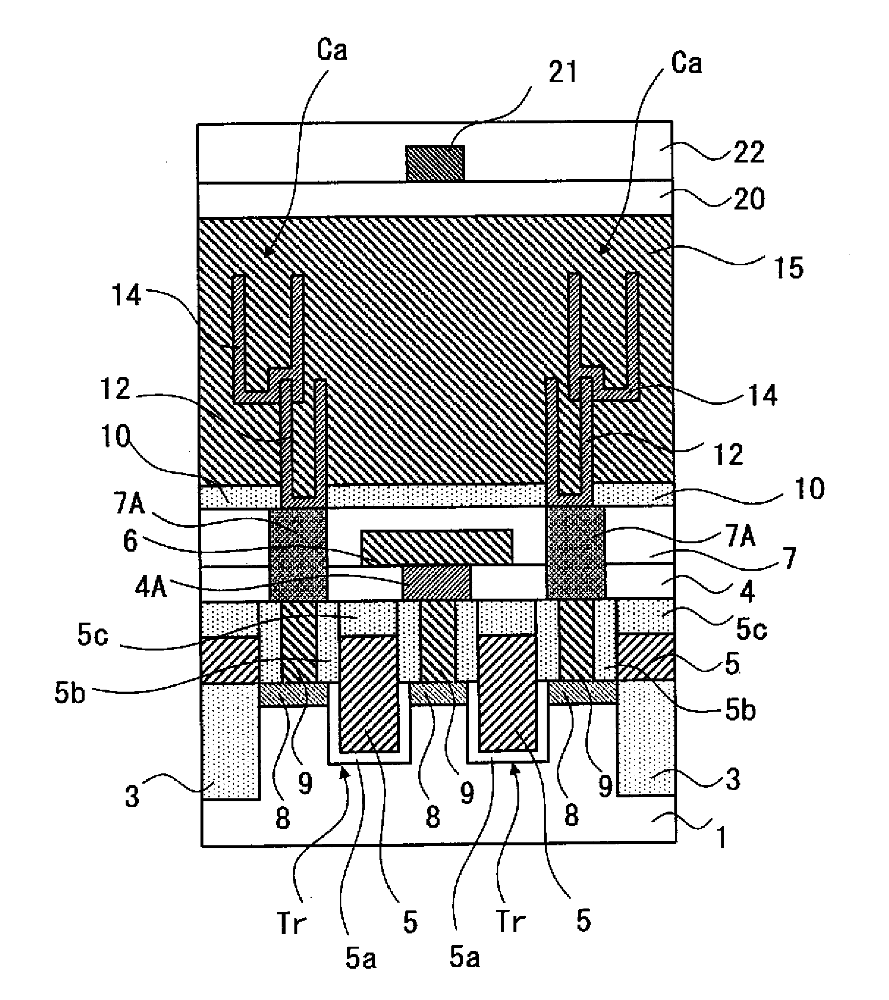
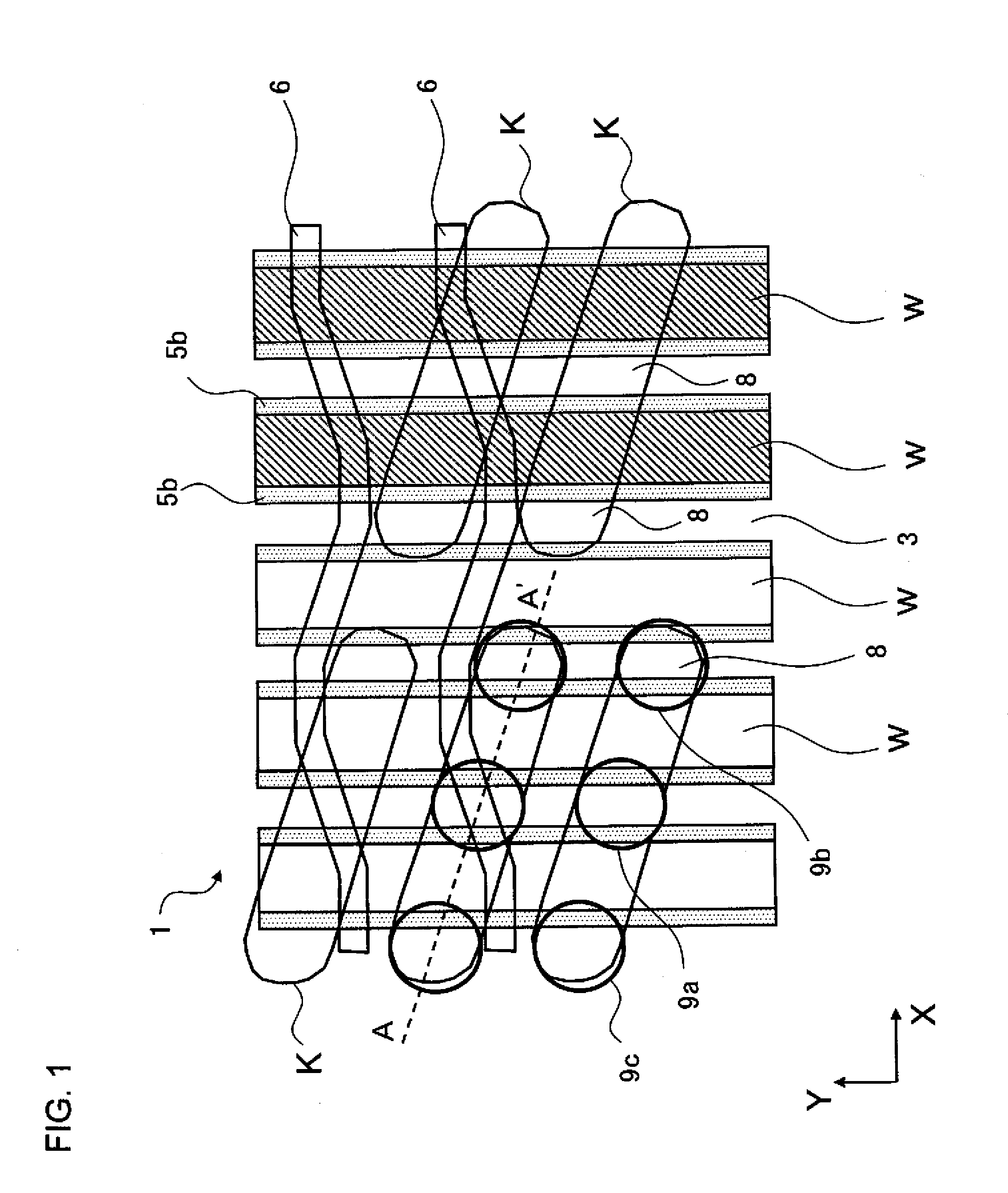
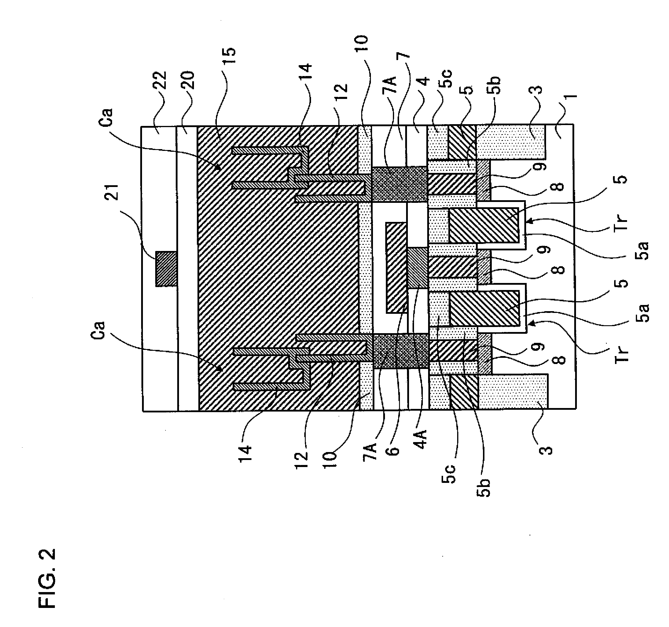
[0048]A semiconductor memory device according to one exemplary embodiment includes: a semiconductor substrate; word lines extending in a Y direction on the semiconductor substrate, the word lines being arranged in an X direction perpendicular to the Y direction and being parallel to one another; active regions each elongating in a belt-like manner and intersecting with two of the word lines, the active regions being arranged in the Y direction and being parallel to one another on the semiconductor substrate; capacitance contact plugs respectively connected to one and the other ends of each of the active regions in the longitudinal direction thereof; a stack lower electrode including a first lower electrode formed on each of the capacitance contact plugs and a second lower electrode formed on the first lower electrode; a capacitance insulating film formed on the stack lower electrode; and an upper electrode formed on the stack lower electrode with an intervention of the capacitance i...


PUM


Abstract

A semiconductor memory device including: word lines extending in a Y direction on a semiconductor substrate, the word lines being arranged in an X direction perpendicular to the Y direction and being parallel to one another; active regions each elongating and intersecting with two of the word lines, the active regions being arranged in the Y direction and being parallel to one another on the semiconductor substrate; a capacitance contact plug connected to each end of each of the active regions in the longitudinal direction thereof; a stack lower electrode including a first lower electrode formed on the capacitance contact plug and a second lower electrode formed on the first lower electrode; a capacitance insulating film; and an upper electrode, wherein the center position of the second lower electrode is shifted in a predetermined direction from the center position of the first lower electrode.

Description

BACKGROUND OF THE INVENTION[0001]1. Field of the Invention[0002]The present invention relates to a semiconductor memory device.[0003]2. Description of Related Art[0004]Along with an advance in the miniaturization of semiconductor devices, the area of a memory cell constituting a DRAM (Dynamic Random Access Memory) has also diminished. Accordingly, it is practiced to form a capacitor constituting the memory cell into a three-dimensional shape, in order to ensure sufficient electrostatic capacitance for the capacitor. Specifically, the lower electrode of the capacitor is processed into a cylindrical shape (cylindrical capacitor) or a pillar shape (columnar capacitor) and the capacitor is formed by utilizing the sidewalls thereof, thereby increasing the surface area of the electrode.[0005]Due to a reduction in the area of the memory cell, however, the bottom area of the capacitor lower electrode has also diminished. Accordingly, a hole having a high aspect ratio needs to be formed in a...

Claims


Application Information

Patent Timeline
Patent Type & Authority Applications(United States)
IPC IPC(8): H01L27/108
CPCH01L27/10814H01L28/90H01L27/10873H10B12/315H10B12/05
Inventor YUKI, KAZUYOSHI
Owner ELPIDA MEMORY INC
Why Eureka
Try Eureka