Electro-optical device and electronic apparatus

a technology of optical devices and electronic devices, applied in semiconductor devices, capacitors, instruments, etc., can solve problems such as malfunctioning of pixel transistors

Active Publication Date: 2020-09-01
SEIKO EPSON CORP
View PDF13 Cites 0 Cited by
  • Summary
  • Abstract
  • Description
  • Claims
  • Application Information

AI Technical Summary

Benefits of technology

[0004]In view of the above, an advantage of some aspects of the invention is that an electro-optical device configured to prevent electrical coupling from occurring between the gate and the drain, even when a holding capacitance is formed with a recess section in a region overlapping with a gate electrode in a plan view, and an electronic apparatus are provided.
[0006]As described above, the first holding capacitance is formed by the first capacitance electrode, the first dielectric layer, and the second capacitance electrode that overlap on the bottom, the inner walls, and the like of the first recess section formed in the second inter-layer insulation film, and thus a large electrostatic capacitance can be achieved even when an occupied planer area is small. With this configuration, the second inter-layer insulation film needs to be thick and thus the first inter-layer insulation film needs to be thin. Still, the first capacitance line is formed on the surface of the first inter-layer insulation film on the side of the pixel electrode, and the first capacitance line shields a section between the second capacitance electrode to which the drain potential is applied and the gate electrode. This can prevent an occurrence of electrical coupling between the gate and the drain.
[0011]The invention may employ an aspect in which the first scan line extends in the first direction between the semiconductor layer and the first inter-layer insulation film, and the first capacitance line extends in the first direction to overlap with the first scan line in a plan view. With the invention, an occurrence of the electrical coupling is prevented between the first scan line and the electrode to which a drain potential is applied. Thus, the first capacitance line and the first scan line can be used for shielding the semiconductor layer from light from the side of the pixel electrode.

Problems solved by technology

This coupling might lead to malfunctioning of the pixel transistor and thus is not preferable.

Method used


Image

  • Electro-optical device and electronic apparatus
  • Electro-optical device and electronic apparatus
  • Electro-optical device and electronic apparatus

Examples


Embodiment Construction

[0030]Exemplary embodiments of the invention will be described with reference to the accompanying drawings. Meanwhile, in the drawings which are referred to in the description below, each layer and each member are illustrated in sizes which can be recognized in the drawing, and thus the scales thereof are different for each layer and each member. In addition, in the description below, when a layer which is formed on a first side substrate is described, an upper layer side or a surface side means a side opposite to a side on which the substrate is positioned (or means a side on which a second side substrate is positioned), and a lower layer side means a side on which the substrate is positioned.

Configuration of Electro-optical Device

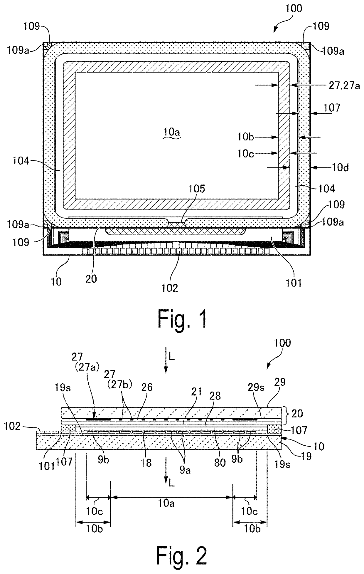
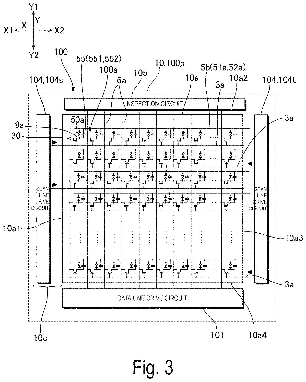
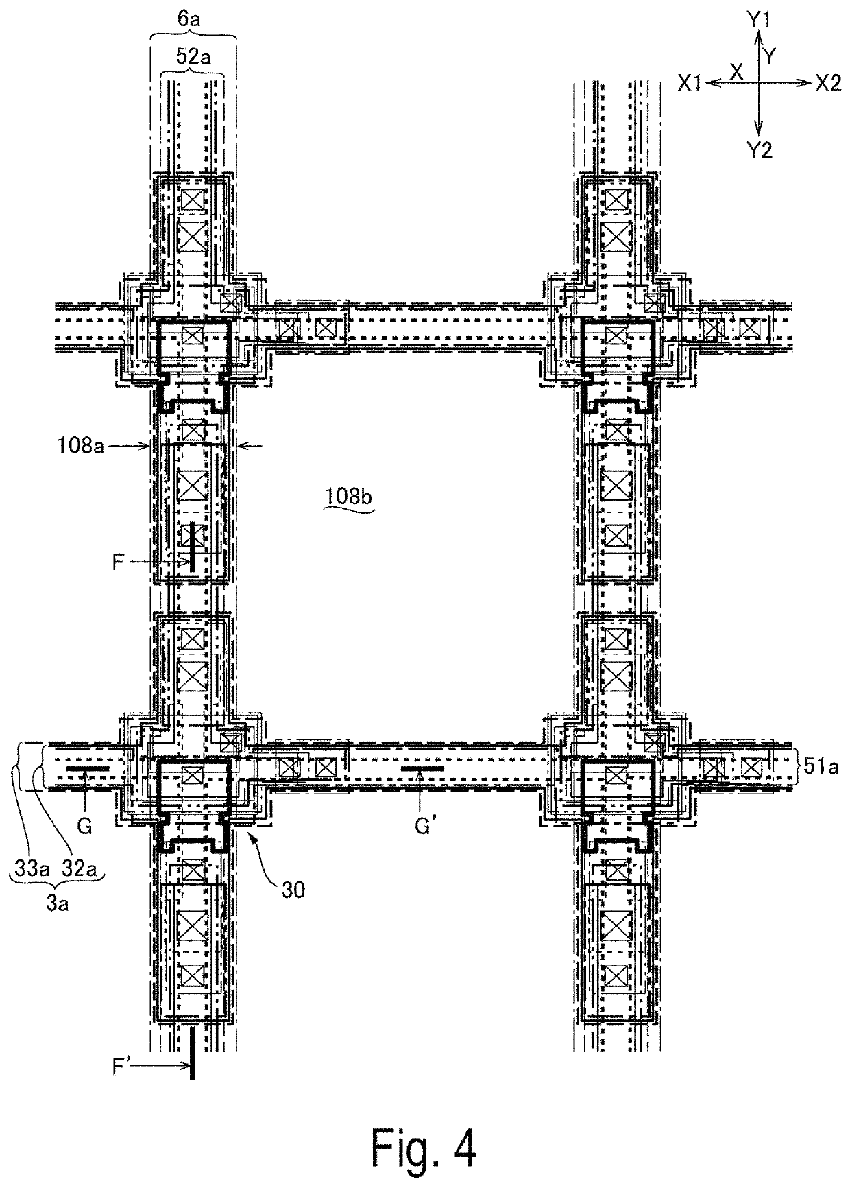
[0031]FIG. 1 is a plan view illustrating an electro-optical device 100 to which the invention is applied. FIG. 2 is a cross-sectional view illustrating the electro-optical device 100 illustrated in FIG. 1. As illustrated in FIG. 1 and FIG. 2, in the elect...


PUM

PropertyMeasurementUnit
capacitanceaaaaaaaaaa
holding capacitanceaaaaaaaaaa
semiconductoraaaaaaaaaa

Abstract

On the first side substrate of an electro-optical device, a first maintenance capacitance is formed by a first capacitance electrode, a first dielectric layer, and a second capacitance electrode overlapped with each other on a bottom and an inner walls of a first recess section formed in an inter-layer insulation film. The inter-layer insulation film needs to be thick and thus an inter-layer insulation film needs to be thin. A first capacitance line is formed on a surface of the inter-layer insulation film on the side of a pixel electrode. Thus, the first capacitance line shields a section between a gate electrode and the second capacitance electrode to which a drain potential is applied.

Description

BACKGROUND1. Technical Field[0001]The invention relates to an electro-optical device provided with a pixel transistor and a holding capacitance on a first side substrate, and to an electronic apparatus.2. Related Art[0002]An electro-optical device (liquid crystal apparatus) which is used as the light valve of a transmission-type display apparatus and the like includes a first side substrate, on which a pixel transistor and a maintenance capacitance are formed, a second side substrate, on which a counter electrode is formed, and an electro-optical layer (liquid crystal layer) arranged between the first side substrate and the counter electrode. In the electro-optical device, the first side substrate has a scan line formed on the side of a pixel electrode relative to a semiconductor layer of the pixel transistor. A part of the scan line constitutes a gate electrode. A holding capacitance is constituted by a drain electrode (lower electrode), a dielectric layer, and a capacitance line (...

Claims


Application Information

Patent Timeline
Patent Type & Authority Patents(United States)
IPC IPC(8): G02F1/1362H01L29/786G02F1/1343H01L27/12H01L49/02G02F1/1368G02F1/1333H01L29/417H01L29/423
CPCH01L29/41733G02F1/136213G02F1/136286H01L29/78672H01L27/124H01L27/1255H01L28/60H01L29/42384G02F1/1368H01L27/1248G02F1/133345H01L29/78633G02F1/134309H01L29/78648G02F1/136209G02F2001/136218H01L29/78675G02F2001/13685G02F2203/01G02F2202/104G02F1/136227G02F1/136218G02F1/13685
Inventor IZAWA, SHOTAROITO, SATOSHI
Owner SEIKO EPSON CORP
Why Eureka
Try Eureka