Printed circuit board for optical waveguides and method of manufacturing the same

Inactive Publication Date: 2011-01-27
SAMSUNG ELECTRO MECHANICS CO LTD
View PDF1 Cites 2 Cited by
  • Summary
  • Abstract
  • Description
  • Claims
  • Application Information

AI Technical Summary

Benefits of technology

[0044]As described above, with the printed circuit board for optical waveguides and the method of manufacturing the same according to the present invention, the circuit patterns formed on the side substrate are positioned at the central part in the thickness direction of the printed circuit board for optical waveguides as compared to the core of the optical waveguide, thereby making it possible to minimize the effect of stress on the circuit patterns when the printed circuit

Problems solved by technology

However, the printed circuit board including the existing optical waveguides has low bending reliability since

Method used


Image

  • Printed circuit board for optical waveguides and method of manufacturing the same
  • Printed circuit board for optical waveguides and method of manufacturing the same
  • Printed circuit board for optical waveguides and method of manufacturing the same

Examples


first embodiment

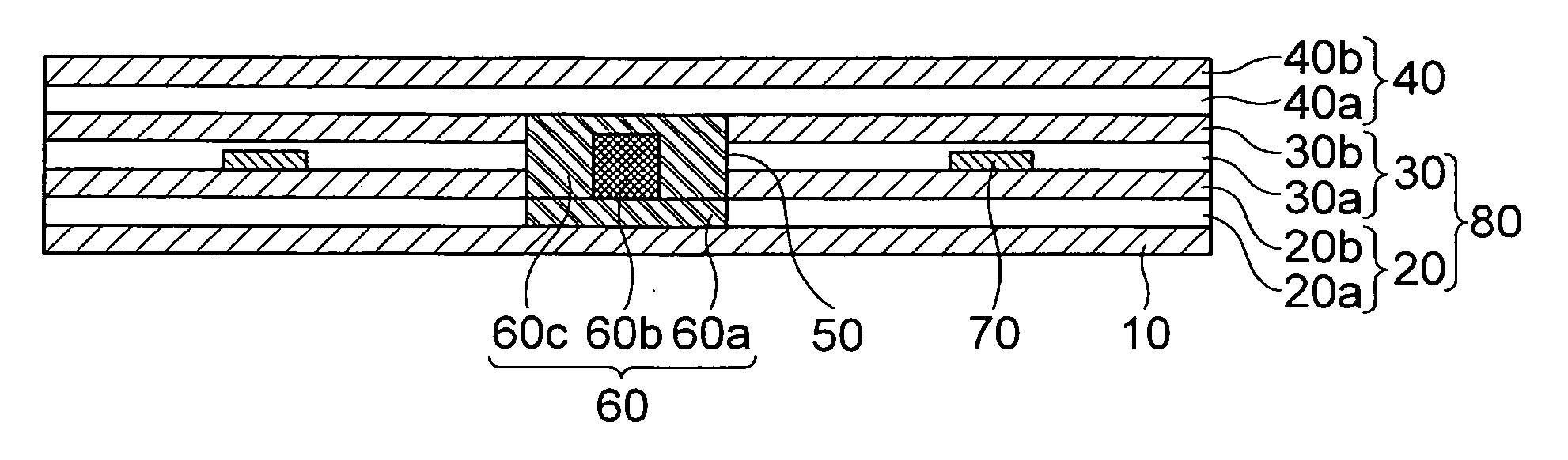
[0059]First, the printed circuit board for optical waveguides according to the present invention includes a base substrate 10, an optical waveguide 60 that is formed on an upper middle of the base substrate 10, and a side substrate 80 that is formed on the base substrate 10, has a through hole 50, through which the optical waveguide 60 penetrates, at a middle thereof, and has a first circuit pattern 70 formed inside the side substrate 80, as shown in FIGS. 1 and 2.

[0060]An upper substrate 40 is formed on the side substrate 80 including the optical waveguide 60. Herein, the upper substrate 40 may not be formed.

[0061]The base substrate 10 may be made of an insulating layer such as polyimide, etc. In addition, the base substrate 10 may be made of a metal foil, such as a copper foil (Cu foil), etc., instead of the insulation layer or may be made of a laminate material of the insulating layer and the metal foil, etc.

[0062]The optical waveguide 60 formed on the base substrate 10 includes ...

second embodiment

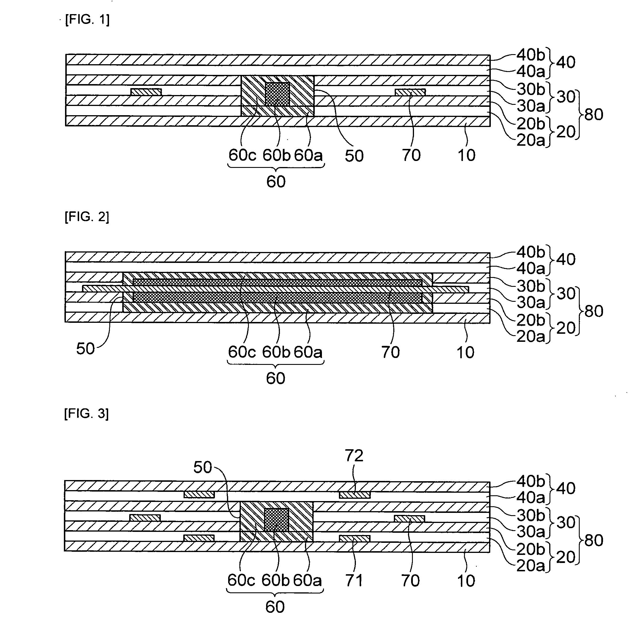
[0080]Next, a printed circuit board for optical waveguides according to the present invention will be described in detail with reference to FIG. 3.

[0081]As shown in FIG. 3, a configuration of the printed circuit board for optical waveguide according to the second embodiment of the present invention is approximately similar to the configuration of the printed circuit board of optical waveguides according to the first embodiment of the present invention. However, the second embodiment is different from the first embodiment only in that it further includes a second circuit pattern 71 formed inside the side substrate 80 and having a lower surface contacting the upper surface of the base substrate 10.

[0082]Herein, the second circuit pattern 71 may be formed inside the first adhesive layer 20a configuring the side substrate 80.

[0083]Further, the printed circuit board for optical waveguides according to the second embodiment of the present invention may further include a third circuit patt...

third embodiment

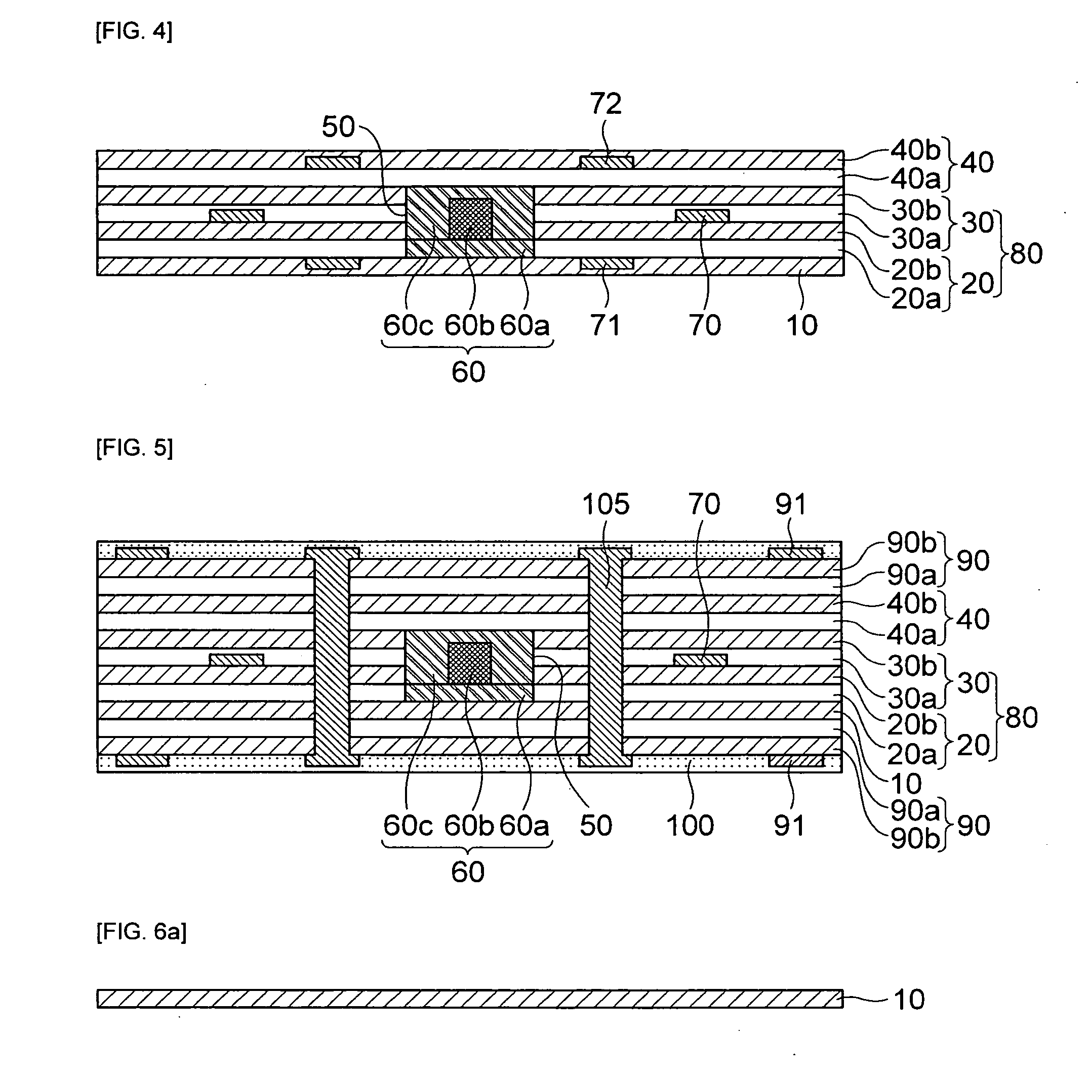
[0085]Next, the printed circuit board for optical waveguides according to the present invention will be described in detail with reference to FIG. 4.

[0086]As shown in FIG. 4, a configuration of the printed circuit board for optical waveguide according to the third embodiment of the present invention is approximately similar to the configuration of the printed circuit board of optical waveguides according to the second embodiment of the present invention. However, the fourth embodiment is different from the first embodiment only in that the second circuit pattern 71 is formed inside the base substrate 10, instead of being formed inside the side substrate.

[0087]In other words, according to the third embodiment of the present invention, the second circuit pattern 71 may be formed inside the base substrate 10 and the upper surface of the second circuit pattern 71 may contact the lower surface of the side substrate 80.

[0088]Further, the printed circuit board for optical waveguides accord...


PUM

PropertyMeasurementUnit
Thicknessaaaaaaaaaa
Adhesivityaaaaaaaaaa
aaaaaaaaaa

Abstract

The present invention relates to a printed circuit board for optical waveguides and a method of manufacturing the same. The present invention provides a printed circuit board for optical waveguides includes: a base substrate; an optical waveguide that is formed on an upper middle of the base substrate and includes a lower clad, a core formed on an upper middle of the lower clad, and an upper clad formed on the lower clad to surround an upper surface and a side surface of the core; and a side substrate that is formed on the base substrate and has a through hole, through which the optical waveguide penetrates, provided at the middle thereof and a circuit pattern formed therein and a method of manufacturing a printed circuit board for optical waveguides.

Description

CROSS REFERENCES RELATED APPLICATIONS[0001]The present application claims priority under 35 U.S.C. 119 and 35 U.S.C. 365 to Korean Patent Application No. 10-2009-0067510 filed on Jul. 23, 2009, which is hereby incorporated by reference in its entirety.BACKGROUND OF THE INVENTION[0002]1. Field of the Invention[0003]The present invention relates to a printed circuit board for optical waveguides and a method of manufacturing the same, and more specifically, to a printed circuit board for optical waveguides wherein a center in a thickness direction of the printed circuit board for optical waveguides is formed with a circuit pattern and a method of manufacturing the same.[0004]2. Description of the Related Art[0005]Generally, a printed circuit board (PCB) means a circuit board wherein various kinds of many parts are densely mounted on a panel of phenol resin or epoxy resin and circuits connecting between each part are compressed and fixed on a surface of the panel made of resin.[0006]Suc...

Claims


Application Information

Patent Timeline
IPC IPC(8): G02B6/12B29C65/48H05K3/36
CPCB32B2307/51B32B2457/08C07D301/06G02B6/138G02B6/43Y10T29/49126H05K1/028H05K3/281H05K3/4635H05K2203/063Y10T156/10H05K1/0274G02B6/12
Inventor KIM, SANG HOONCHO, HAN SEOJUNG, JAE HYUNKIM, JOON SUNG
Owner SAMSUNG ELECTRO MECHANICS CO LTD
Why Eureka
Try Eureka