Semiconductor device and method for fabricating the same

a technology of semiconductors and components, applied in the direction of semiconductor devices, basic electric elements, electrical equipment, etc., can solve the problems of difficult to reduce a whole size, and achieve the effect of reducing a contact resistan

Inactive Publication Date: 2011-02-03
SK HYNIX INC
View PDF6 Cites 2 Cited by
  • Summary
  • Abstract
  • Description
  • Claims
  • Application Information

AI Technical Summary

Benefits of technology

[0006]Embodiments of the present invention provide a semiconductor memory device and a fabricating method of the same capable of preventing a self aligning contact (SAC) fail and a gate induced drain leakage (GIDL) phenomenon and reducing a contact resistance by forming a dummy gate on a buried gate for the dummy gate to act as an etching barrier when a landing plug contact hole is formed.

Problems solved by technology

In case of a complex semiconductor memory device, it is difficult to reduce a whole size due to a plurality of transistors included in the semiconductor memory device.

Method used


Image

  • Semiconductor device and method for fabricating the same
  • Semiconductor device and method for fabricating the same
  • Semiconductor device and method for fabricating the same

Examples


Embodiment Construction

[0030]Hereinafter, a contact plug for a buried gate of a semiconductor device and a manufacturing method for the same in accordance with an embodiment of the present invention are described in detail with reference to the accompanying drawings.

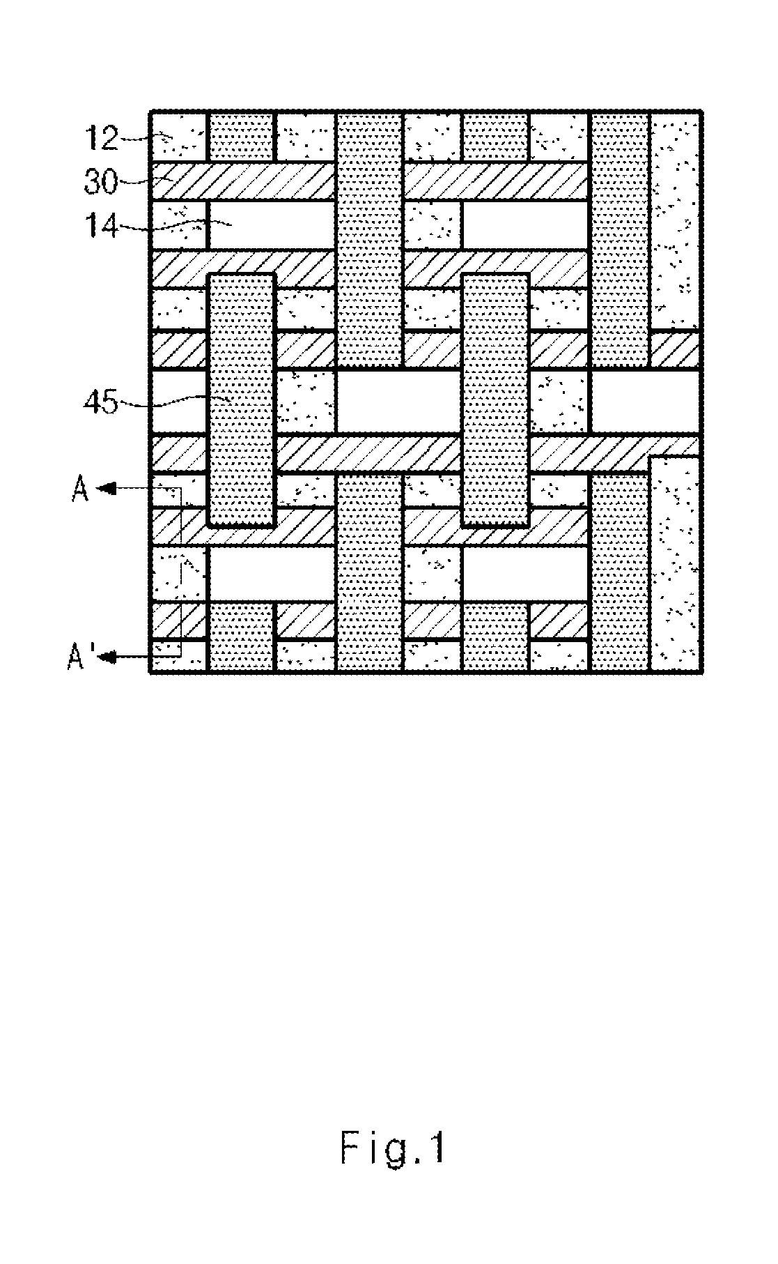
[0031]FIG. 1 is a plan view illustrating a semiconductor device in accordance with the present invention. Referring to FIG. 1, a plurality of active regions 12 is formed in a vertical direction on a semiconductor substrate 10, and a device isolation film 14 for defining the active region 12 is formed on the semiconductor substrate 10.

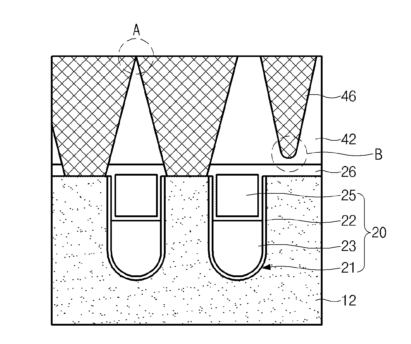
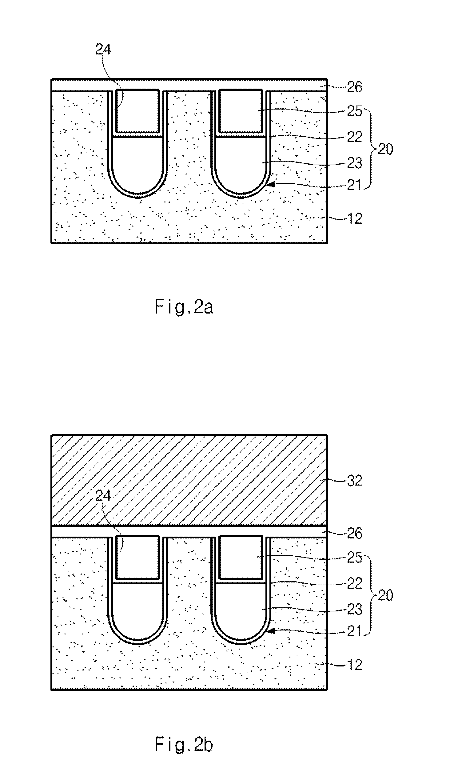
[0032]A plurality of buried gates 20 (refer to FIG. 2A) is formed in a horizontal direction across the plurality of active regions 12. This buried gate 20 is formed such that two buried gates 20 cross one active region 12. On an upper part of the buried gate 20, a dummy gate 30 is formed at the same position as the buried gate 20 in a plan view. Although the dummy gate 30 does not act as an actual gate, it acts as...


PUM


Abstract

A semiconductor device comprises a buried gate formed by being buried under a surface of a semiconductor substrate, a dummy gate formed on the buried gate, and a landing plug formed on a junction region of the semiconductor substrate being adjacent to the dummy gate.

Description

CROSS-REFERENCE TO RELATED APPLICATION[0001]The priority based on Korean patent application No. 10-2009-0069072 filed on 28 Jul. 2009, the disclosure of which is hereby incorporated in its entirety by reference, is claimed.BACKGROUND OF THE INVENTION[0002]The present invention relates to a semiconductor device, and more specifically, to a semiconductor device including a buried gate and a fabricating method of the same.[0003]A typical semiconductor memory device is a dynamic random access memory (DRAM). A DRAM device includes a plurality of unit cells each of which includes a capacitor and a transistor. The capacitor is used for temporarily storing data and the transistor is used for transferring the data between a bit line and the capacitor in response to a control signal (word line). The transistor has three regions, i.e., a gate, a source and a drain. According to a control signal inputted to the gate, an electric charge moves between the source and the drain. The movement of the...

Claims


Application Information

Patent Timeline
Patent Type & Authority Applications(United States)
IPC IPC(8): H01L29/78H01L21/28H01L21/3205
CPCH01L29/66621H01L21/76897H01L21/02225H01L21/2254H01L21/2255H01L21/4763H01L29/66348
Inventor HONG, SUNG PYO
Owner SK HYNIX INC
Why Eureka
Try Eureka