Self-timed write boost for SRAM cell with self mode control

a write boost and self-timed technology, applied in the field of sram cells, can solve the problems of data corruption, many problems in sram memory, write failure in sram memory cells, etc., and achieve the effect of less boost and good writability

Active Publication Date: 2011-02-03
STMICROELECTRONICS INT NV
View PDF9 Cites 14 Cited by
  • Summary
  • Abstract
  • Description
  • Claims
  • Application Information

AI Technical Summary

Benefits of technology

[0012]According to the present invention, the write boost circuit provides an automatic mode control for boost with different modalities (with respect to the external supply voltage and also with respect to the extent of boost required at different process corners). The method of the present invention also takes care of the minimum boost provided to process corners with good writability where less boost is required. The boost is realized in terms of ground raising in the particular context and in general applicable to all other methods. A reduction of 50% to 75% in boost power at PVTs (i.e., process / supply voltage / temperatures) where boost is not required was observed. The self mode control with respect to supply voltage helps to gain in boost power 30% to 50%.

Problems solved by technology

In deep submicron technology, worst process conditions and voltage scaling has created many problems in SRAM memories.
Write failure in an SRAM memory cell is one critical problem caused due to the above reasons.
If the driver transistor resistance is comparable to the pass transistor resistance, then the raised internal node level can trip the memory cell in the opposite direction and thus the data will be corrupted.
This leads to further degrading of writability and the write time of the memory cell, because now a high voltage swing is required across BL / BLB for raising the level of the stored zero.
This makes the writability issue even more of a concern at very low voltages.
At these low voltage levels, SRAM cell designs are tuned for ensuring margins but the writability of the memory cell is major problem.
Writability is a problem at a slow NMOS and fast PMOS process corner.
The disadvantages of this technique are that the GND of the complete row is raised, which reduces the signal to noise margin of unselected MUX columns of the same row.
The disadvantages are that the VDD lowering / cut off is implemented for both PMOS transistors simultaneously.

Method used


Image

  • Self-timed write boost for SRAM cell with self mode control
  • Self-timed write boost for SRAM cell with self mode control
  • Self-timed write boost for SRAM cell with self mode control

Examples


Embodiment Construction

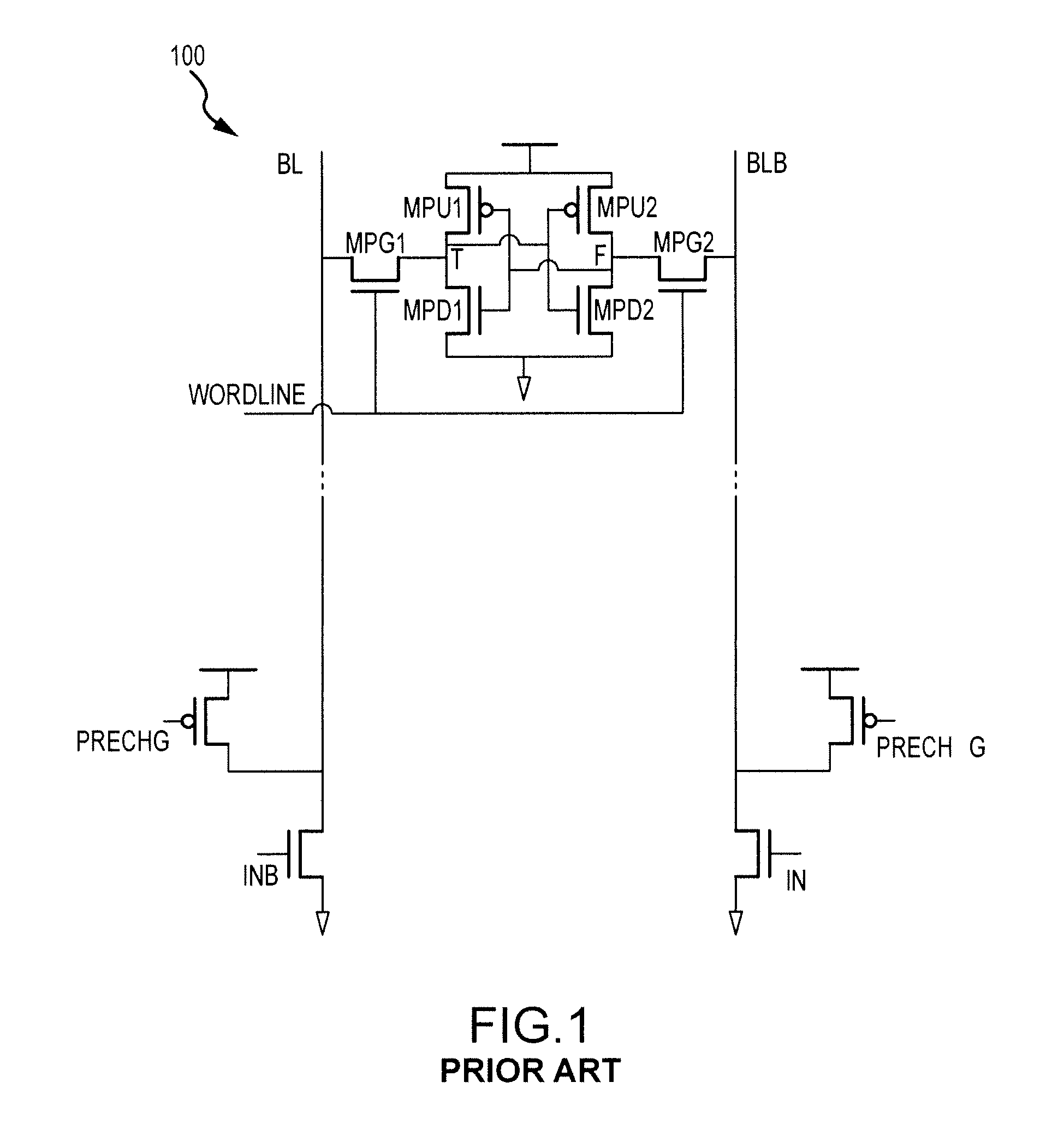
[0019]In a conventional SRAM memory cell, such as memory cell 100 in FIG. 1, there is word line that activates the memory cell read / write operation, precharge block for precharging BL / BLB after read / write operation, and write driver NMOS which is used to pull down BL / BLB in write operation. In / Inb are data inputs and its inverted signal used to write a zero or one depending on data logic.

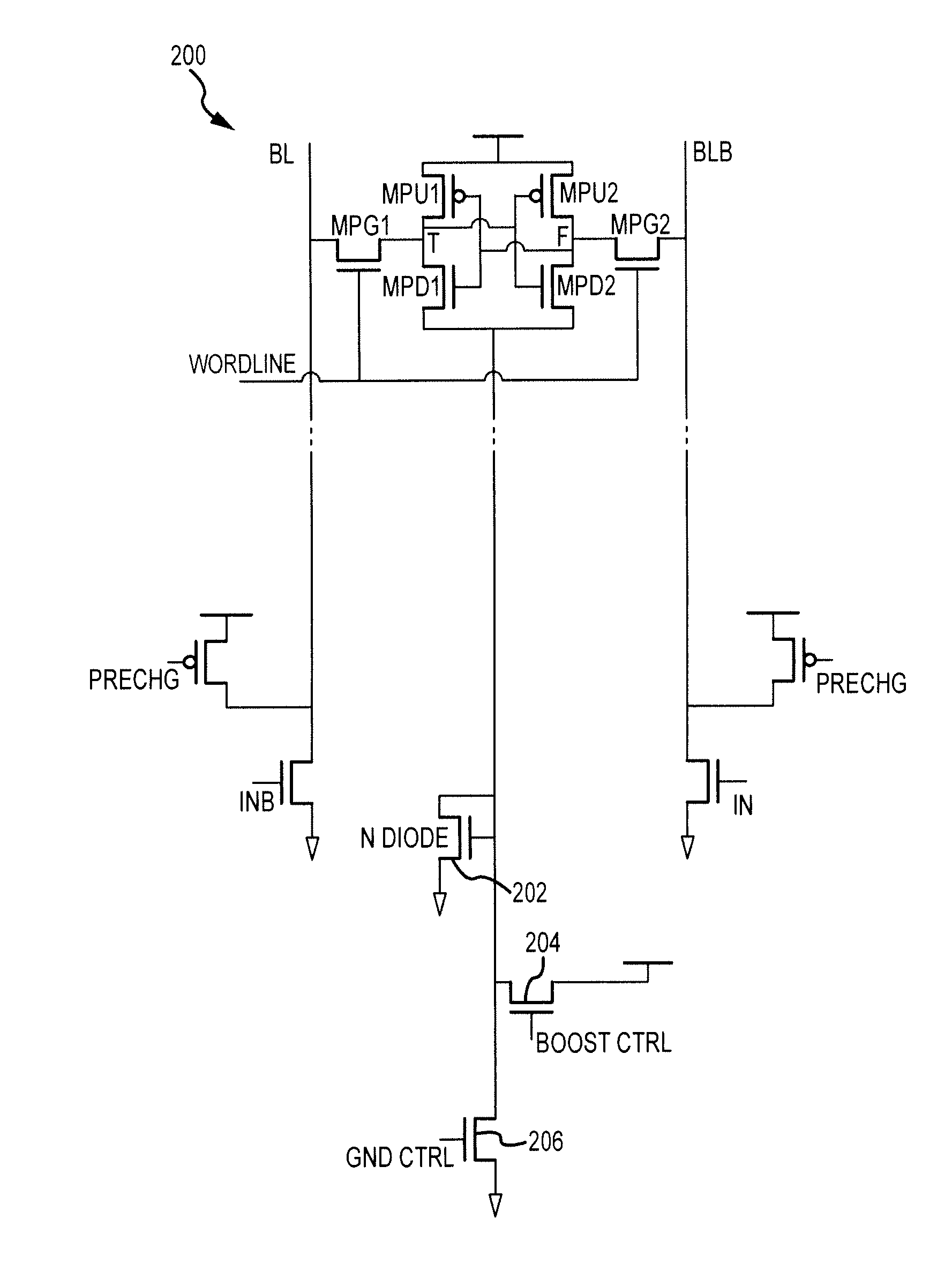
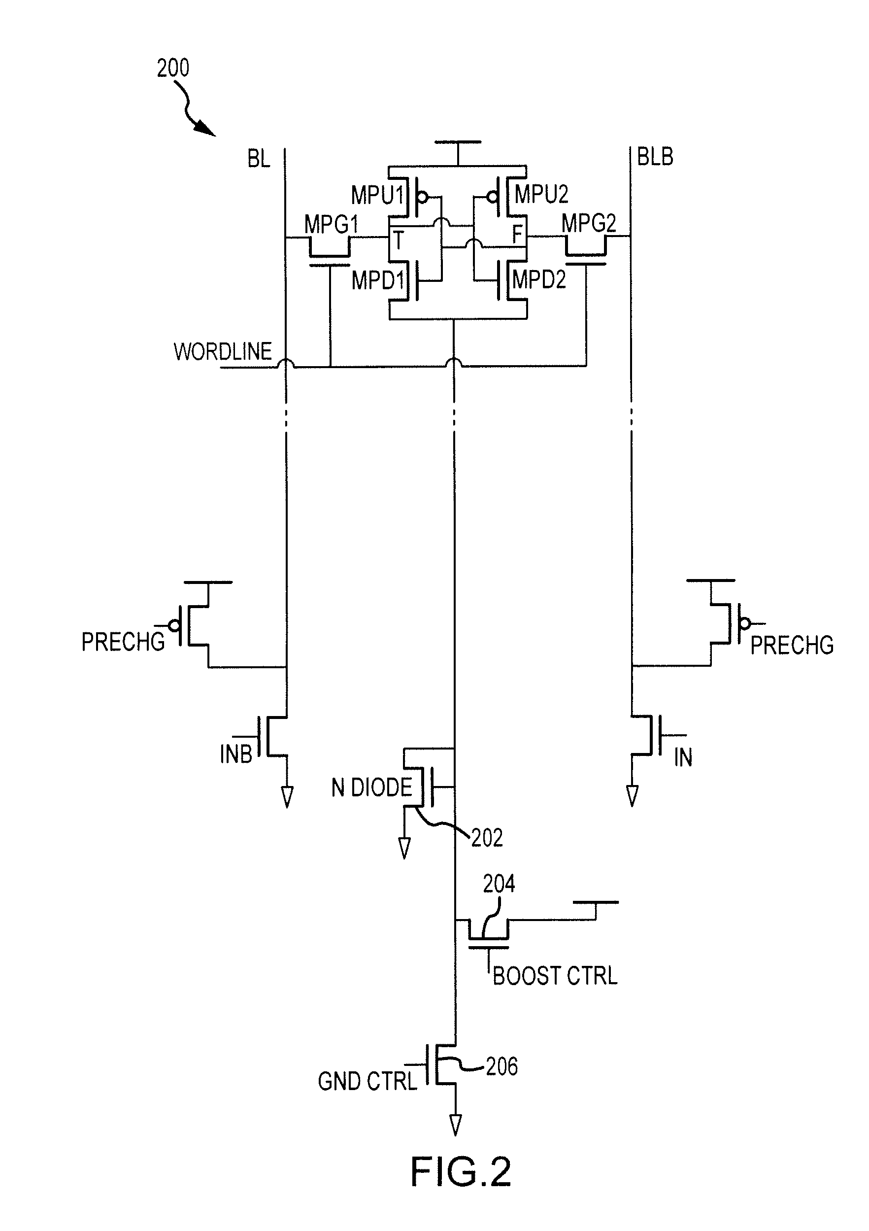
[0020]Referring now to FIG. 2, an SRAM memory 200 includes a write boost circuit coupled to the ground power terminal of an SRAM cell, the write boost circuit including an N-channel diode-connected transistor 202, an N-channel transistor 204, and an N-channel transistor 206. During a write cycle, the GND CTRL Signal is set low, thus cutting off GND to the SRAM memory cell. The boost CTRL signal is then asserted high and thus the GND line of the SRAM memory cell is raised to boost writability. N-diode 202 is used to limit the voltage up to VTnmos. Writability is much poorer due to a slow NMOS pass ga...


PUM


Abstract

A write boost circuit provides an automatic mode control for boost with different modalities with respect to the external supply voltage and also with respect to the extent of boost required at different process corners. The write boost circuit also takes care of the minimum boost provided to process corners with good writability where less boost is required. The boost is realized in terms of ground raising in the particular context and in general applicable to all other methods.

Description

RELATED APPLICATION[0001]The present application claims priority of India Provisional Patent Application No. 1616 / Del / 2009 filed Aug. 3, 2009, which is incorporated herein in its entirety by this reference.FIELD OF THE INVENTION[0002]The present invention relates to SRAM cells, and more particularly, to a write boost circuit to improve the write performance of the SRAM cell.BACKGROUND OF THE INVENTION[0003]In deep submicron technology, worst process conditions and voltage scaling has created many problems in SRAM memories. Write failure in an SRAM memory cell is one critical problem caused due to the above reasons.[0004]During a read operation, the pass transistor and the on NMOS driver act as voltage divider which raises the level of a zero stored in the memory cell. If the driver transistor resistance is comparable to the pass transistor resistance, then the raised internal node level can trip the memory cell in the opposite direction and thus the data will be corrupted. So for a ...

Claims


Application Information

Patent Timeline
Patent Type & Authority Applications(United States)
IPC IPC(8): G11C7/00G11C11/00
CPCG11C11/413G11C5/145
Inventor KUMAR, ASHISHBATRA, NAVEEN
Owner STMICROELECTRONICS INT NV
Why Eureka
Try Eureka