Touch detecting device and method thereof
a technology of touch detection and detection device, which is applied in the field of touch panels, can solve the problems of system misjudgment, increased hardware cost, and difficulty in separating finger touch from noise interference,
- Summary
- Abstract
- Description
- Claims
- Application Information
AI Technical Summary
Problems solved by technology
Method used
Image

Examples
first embodiment
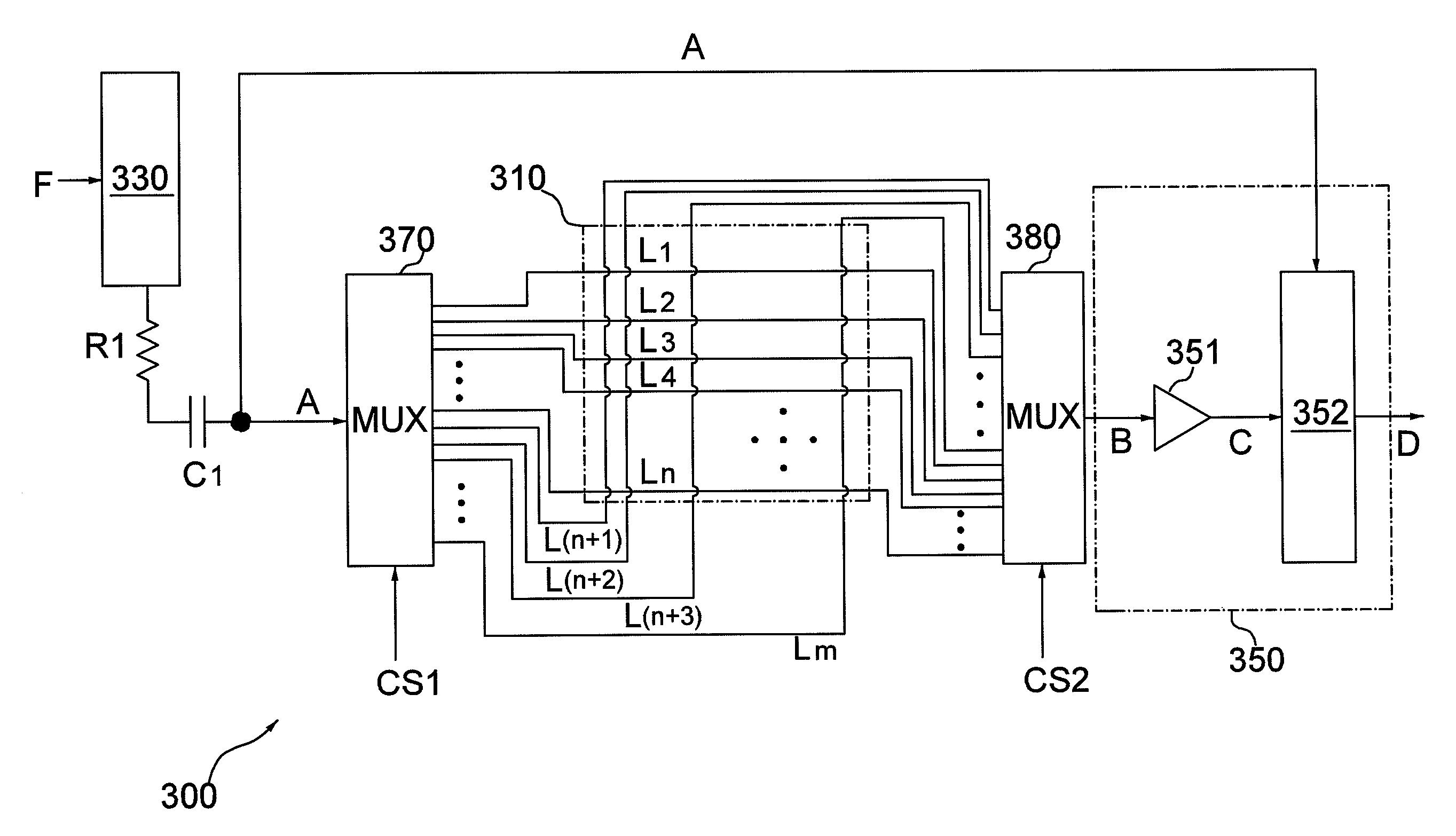
[0050]FIG. 3A is a block diagram of a touch detecting device according to the invention. Referring to FIG. 3A, a touch detecting device 300 of the invention, for use in a touch panel (not shown), includes a conductive line array 310, a driving unit 330, a sensing circuit 350 and two multiplexers 370, 380. In addition, the sensing circuit 350 includes a buffer 351 and a signal extracting unit 352.
[0051]In this embodiment, the conductive line array 310 is formed by a first group of conductive lines L1-Ln on x-axis and a second group of conductive lines L(n+1)-Lm on y-axis that are originally available in the touch panel and arranged in a rectangle pattern (i.e., forming a Cartesian coordinate system), where parameters m and n are positive integers. According to the invention, the originally existing conductive lines of the touch panel are used to detect a capacitive object's touch by means of detecting a current leakage through the capacitive object to the ground. For example, a finge...
second embodiment
[0071]FIG. 6A is a block diagram of a touch detecting device according to the invention. Referring to FIG. 6A, a touch detecting device 600 of the invention, adapted for use in a touch panel (not shown), includes a conductive line array 310, a driving unit 630, a sensing circuit 650 and two multiplexers 670, 680. In addition, the driving circuit 630 includes a random number generator 631 and a random-length wave generator 632 while the sensing circuit 650 includes a differential amplifier 651 and a signal extracting unit 352.
[0072]By way of example without limitation, the random number generator 631 is implemented using a linear feedback shift register in order to generate a sequence of pulses with random time spacings (hereinafter called“the random-length sequence”), e.g., (T1, T2, T3, . . . , Tn). Here, a measurement time interval is given by tm=T1+T2+T3+ . . . +Tn, where T1, T3, T5 . . . denotes time intervals of high voltage levels and T2, T4, T6 . . . denotes time intervals of ...
fifth embodiment
[0093]FIG. 9B is a block diagram of a touch detecting device according to the invention. Referring to FIGS. 6A and 9B, the touch detecting device 600 having a two-port connection configuration uses the driving unit 630 to perform random-length sequence measurement while the touch detecting device 600′ having a single-port connection configuration uses the driving unit 935 to selectively perform the fixed-period sequence measurement or the random-length sequence measurement. Here, the driving unit 935 includes a random number generator 631 and a random-length wave generator 632 and also receives an input fixed frequency F. Accordingly, the driving unit 935 selectively generates either two complementary random-length driving signals A and Ā referenced to a common ground or two complementary fixed-length driving signals A and Ā referenced to a common ground within each measurement time interval tm according to the fixed frequency F or a random-length sequence generated by the random nu...
PUM
 Abstract
Description
Claims
Application Information
 - Generate Ideas
- Intellectual Property
- Life Sciences
- Materials
- Tech Scout
- Unparalleled Data Quality
- Higher Quality Content
- 60% Fewer Hallucinations
Browse by: Latest US Patents, China's latest patents, Technical Efficacy Thesaurus, Application Domain, Technology Topic, Popular Technical Reports.
© 2025 PatSnap. All rights reserved.Legal|Privacy policy|Modern Slavery Act Transparency Statement|Sitemap|About US| Contact US: help@patsnap.com