Light guide array for an image sensor

a light guide array and image sensor technology, applied in the direction of instruments, electric discharge lamps, electrical equipment, etc., can solve the problems of loss of light reception, crosstalk cannot be eliminated, extra cost added to the precise microlens forming process,

Inactive Publication Date: 2011-02-10
TAY HIOK NAM +1
View PDF0 Cites 119 Cited by
  • Summary
  • Abstract
  • Description
  • Claims
  • Application Information

AI Technical Summary

Problems solved by technology

In addition, alignment errors between microlens, color filter, and light guide also contribute to crosstalk.
However, extra cost must be added to the precise microlens forming process, and crosstalk still cannot be eliminated.
Backward reflection from the image sensor at the substrate interface is another issue causing loss of light reception.
This interface can cause undesirable backward reflection away from the sensor.
This approach is not applicable when the interface is silicon substrate and a nitride light guide.

Method used


Image

  • Light guide array for an image sensor
  • Light guide array for an image sensor
  • Light guide array for an image sensor

Examples


Embodiment Construction

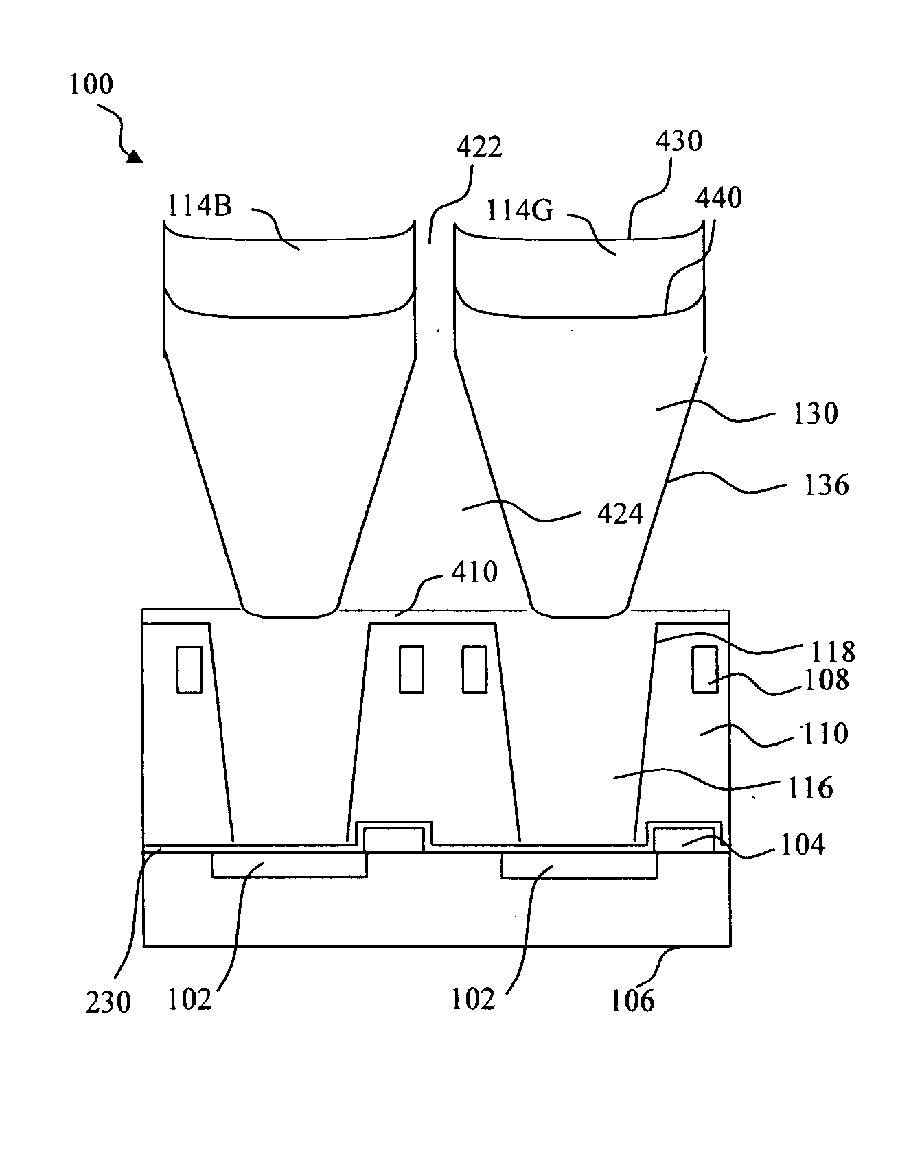
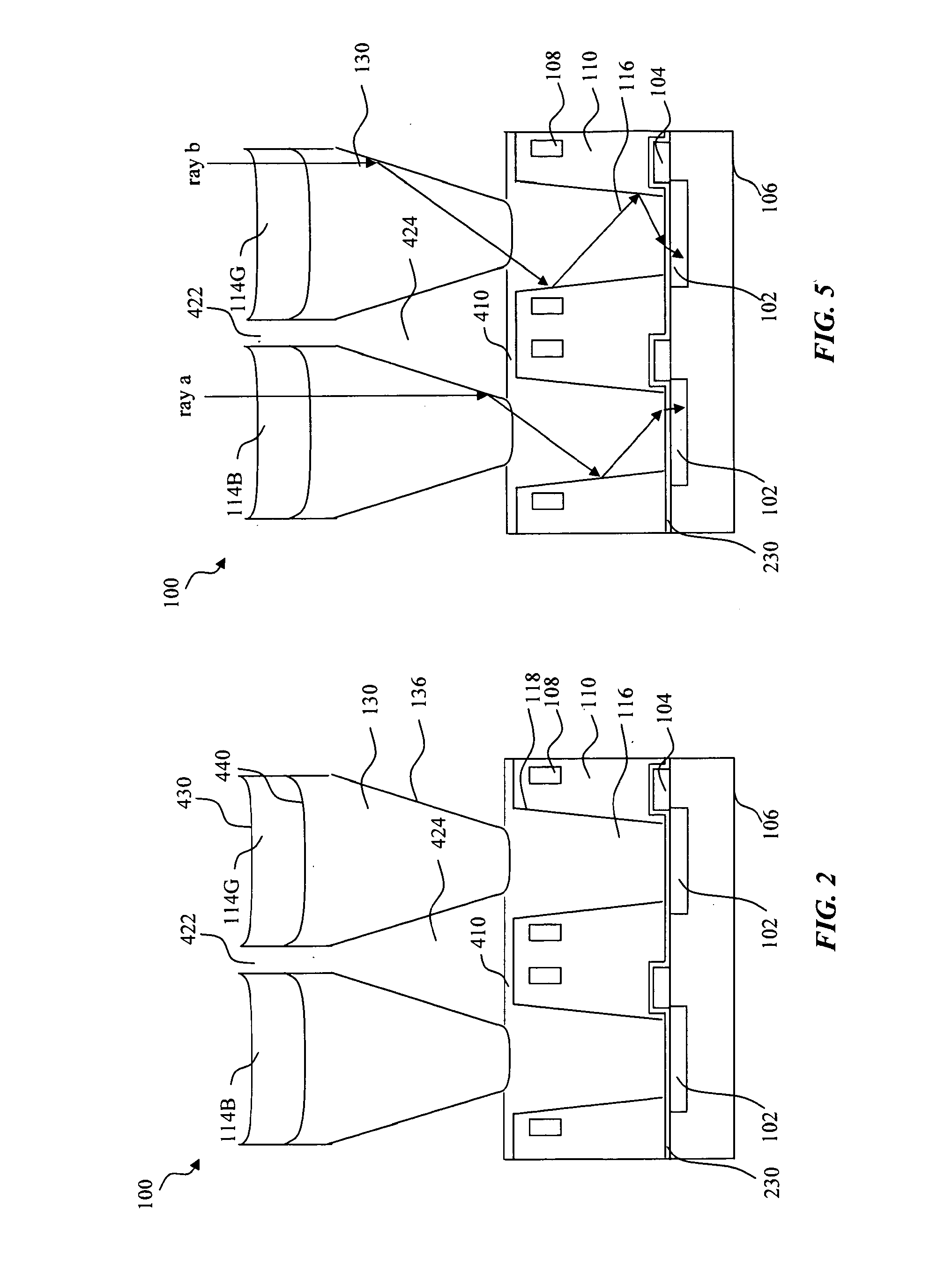
[0048]Disclosed is an image sensor pixel that includes a photoelectric conversion unit supported by a substrate and an insulator adjacent to the substrate. The pixel includes a light guide that is located within an opening of the insulator and extends above the insulator such that a portion of the light guide has an air interface. The air interface improves the internal reflection of the light guide. Additionally, the light guide and an adjacent color filter are constructed with a process that optimizes the upper aperture of the light guide and reduces crosstalk. These characteristics of the light guide eliminate the need for a microlens. Additionally, an anti-reflection stack is constructed above the photoelectric conversion unit and below the light guide to reduce light loss through backward reflection from the image sensor. Two pixels of different color may be individually optimized for anti-reflection by modifying the thickness of one film within the anti-reflection stack.

[0049]...


PUM


Abstract

An image sensor pixel that includes a photoelectric conversion unit supported by a substrate and an insulator adjacent to the substrate. The pixel includes a cascaded light guide that is located within an opening of the insulator and extends above the insulator such that a portion of the cascaded light guide has an air interface. The air interface improves the internal reflection of the cascaded light guide. The cascaded light guide may include a self-aligned color filter having air-gaps between adjacent color filters. Air-gaps may be sealed from above by a transparent sealing film. The transparent sealing film may have a concave surface over the air-gap to diverge light that cross the concave surface into the air-gap away from the air-gap into adjacent color filters. These characteristics of the light guide eliminate the need for a microlens. Additionally, a portion of a support wall between a pair of color filters may have a larger width above than below to form a necking to hold down the color filters for better retention.

Description

BACKGROUND OF THE INVENTION[0001]1. Field of the Invention[0002]The subject matter disclosed, generally relates to structures and methods for fabricating solid state image sensors.[0003]2. Background Information[0004]Photographic equipment such as digital cameras and digital camcorders may contain electronic image sensors that capture light for processing into still or video images. Electronic image sensors typically contain millions of light capturing elements such as photodiodes.[0005]Solid state image sensors can be either of the charge coupled device (CCD) type or the complimentary metal oxide semiconductor (CMOS) type. In either type of image sensor, photo sensors are formed in a substrate and arranged in a two-dimensional array. Image sensors typically contain millions of pixels to provide a high-resolution image.[0006]FIG. 1A shows a sectional view of a prior art solid-state image sensor 1 showing adjacent pixels in a CMOS type sensor, reproduced from U.S. Pat. No. 7,119,319....

Claims


Application Information

Patent Timeline
Patent Type & Authority Applications(United States)
IPC IPC(8): G01J3/51
CPCH01L27/14621H01L27/14623H01L27/14625H01L27/14629H01L27/14685H01L27/14687H01L27/14643
Inventor TAY, HIOK-NAMDO, THANH-TRUNG
Owner TAY HIOK NAM
Why Eureka
Try Eureka