

Laser beam processing machine
a laser beam and processing machine technology, applied in metal-working equipment, welding equipment, manufacturing tools, etc., can solve the problem that the laser beam cannot be precisely directed to a predetermined position
- Summary
- Abstract
- Description
- Claims
- Application Information
AI Technical Summary
Benefits of technology
Problems solved by technology
Method used
Image

Examples
Embodiment Construction
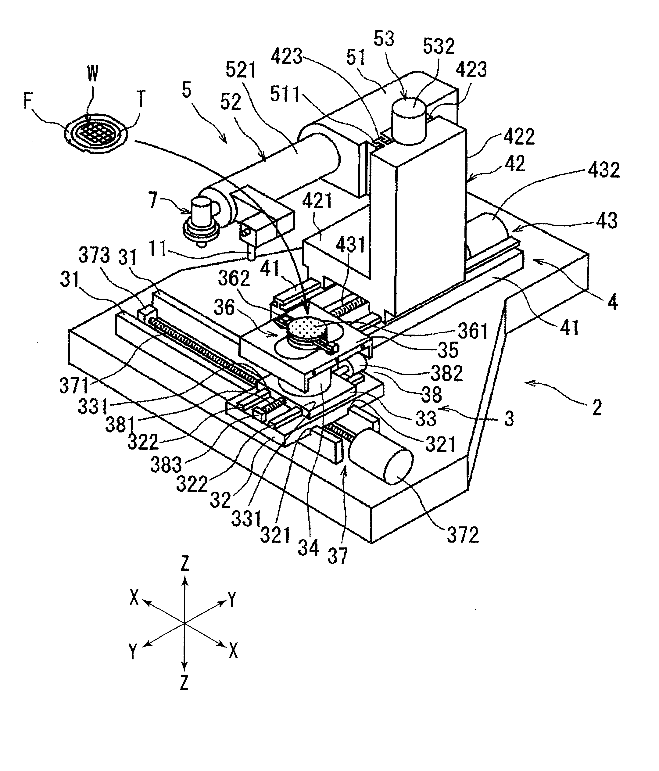
[0019]Preferred embodiments of a laser beam processing machine configured according to the present invention will hereinafter be described in detail with reference to the accompanying drawings. FIG. 1 illustrates a perspective view of the laser beam processing machine configured according to the present invention. The laser beam processing machine illustrated in FIG. 1 includes a stationary base 2; a chuck table mechanism 3; a laser beam irradiation unit support mechanism 4; and a laser beam irradiation unit 5. The chuck table mechanism 3 is disposed on the stationary base 2 shiftably in a processing-transfer direction (X-axial direction) denoted with arrow X so as to hold a workpiece. The laser beam irradiation unit support mechanism 4 is disposed on the stationary base 2 shiftably in an indexing-transfer direction (Y-axial direction) denoted with arrow Y perpendicular to the X-axial direction. The laser beam irradiation unit 5 disposed on the laser beam irradiation unit support me...
PUM
| Property | Measurement | Unit |
|---|---|---|
| cyclic frequency | aaaaa | aaaaa |
| wavelength | aaaaa | aaaaa |
| pressure | aaaaa | aaaaa |
Abstract
Description
Claims
Application Information