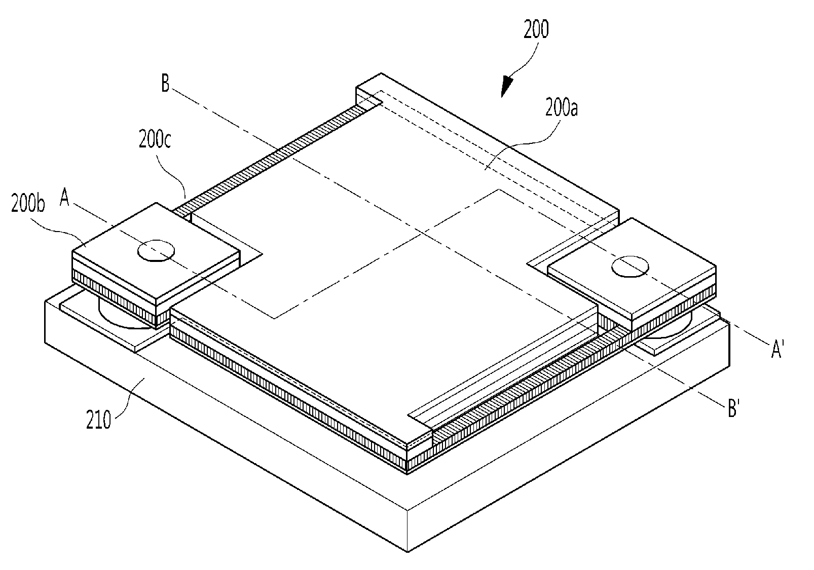
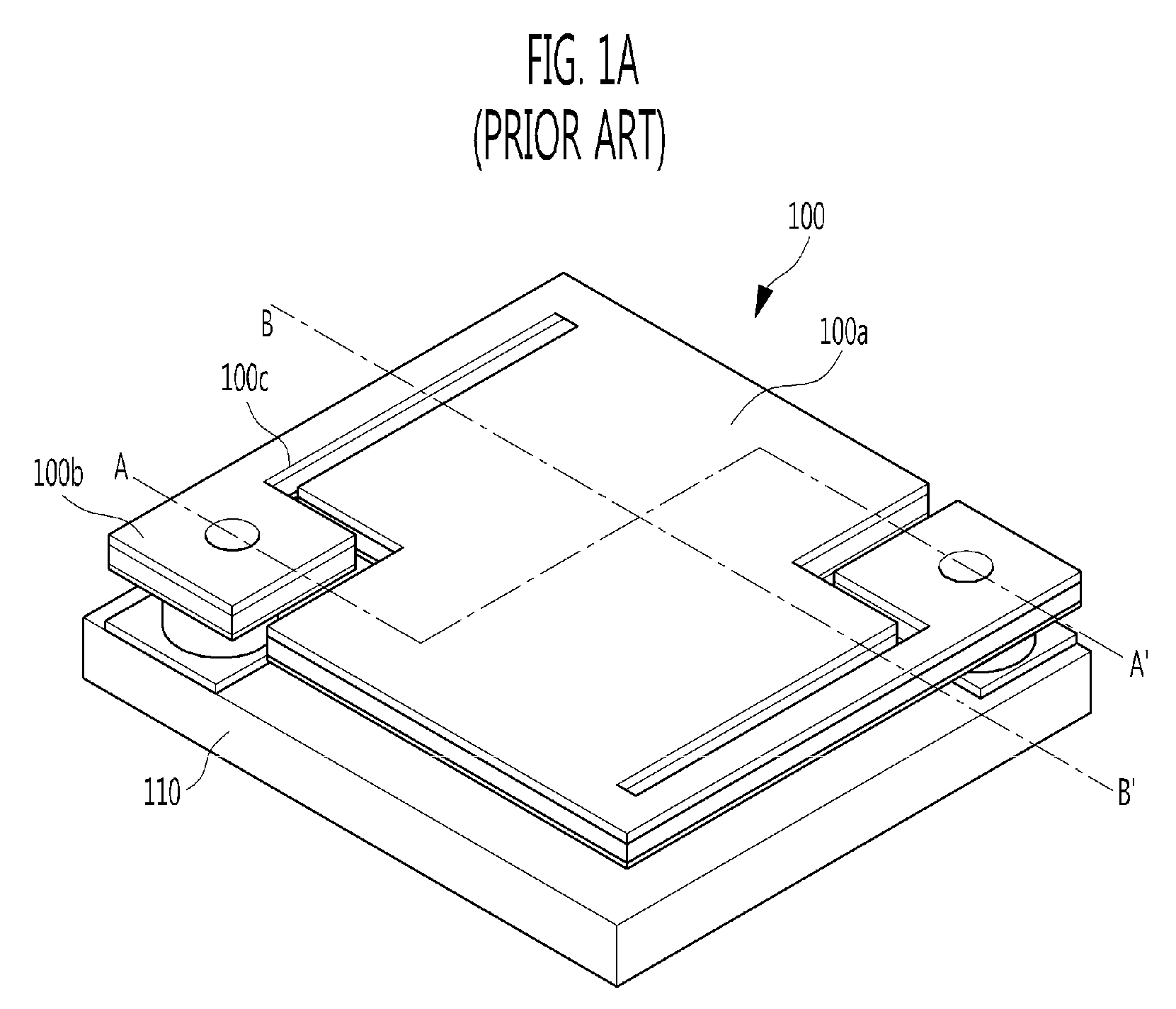
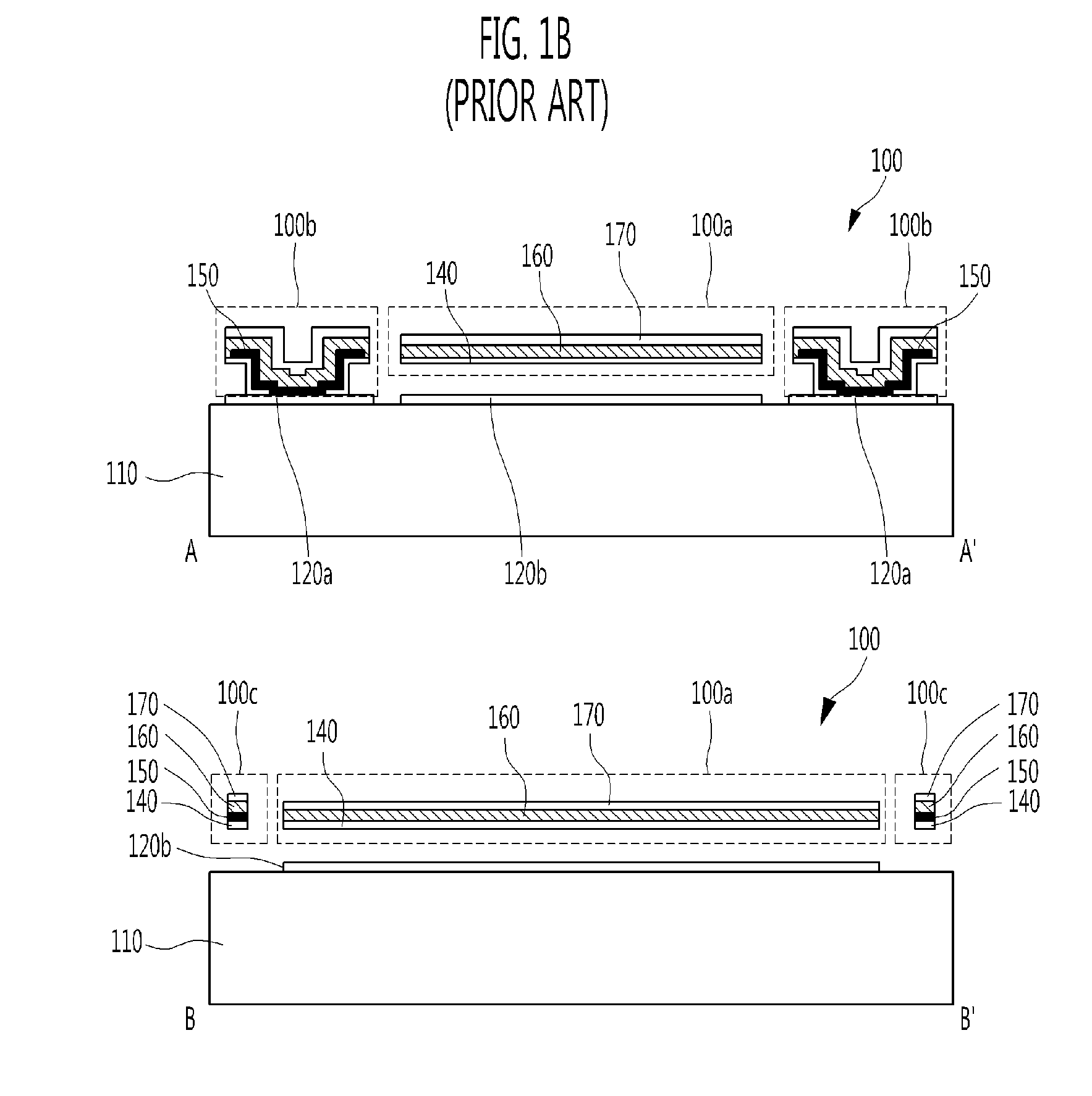
[0020]Hereinafter, exemplary embodiments of the present invention will be described in detail. However, the present invention is not limited to the embodiments disclosed below but can be implemented in various forms. The following embodiments are described in order to enable those of ordinary skill in the art to embody and practice the present invention. When it is determined that the detailed descriptions of a related known function or configuration may make the purpose of the present invention unnecessarily ambiguous in describing the present invention, the detailed descriptions will be omitted here. Throughout this specification, when an element is referred to as “comprising,”“including,” or “having” a component, it does not preclude another component but may further include the other component unless the context clearly indicates otherwise. In the drawings, the thickness of layers and regions may be exaggerated for clarity. When a layer is referred to as being “on” another layer or a substrate, it can be directly formed on the other layer or the substrate or an intervening layer may be present.
[0021]FIG. 2A is a schematic view of an infrared detection sensor according to an exemplary embodiment of the present invention, and FIG. 2B is a cross-sectional view taken along line A-A′ and line B-B′ in FIG. 2A, illustrating the infrared detection sensor shown in FIG. 2A.
[0022]Referring to FIGS. 2A and 2B, an infrared detection sensor 200 according to an exemplary embodiment of the present invention includes a substrate 210 on which a metal pad 220a and a reflection layer 220b are formed; a sensor structure 200a spaced a predetermined distance apart from the reflection layer 220b; an anchor 200b formed on the metal pad 220a and having a predetermined thickness; and a supporting arm 200c extending from the anchor 200b to support the sensor structure 200a.
[0023]A read-out integrated circuit (not shown) is formed in the substrate 210, and the metal pad 200a is electrically connected to the read-out integrated circuit.
[0024]The sensor structure 200a includes a sensing layer 260 with a resistance value varied according to a change in temperature caused when infrared is absorbed, and a lower protection layer 240 and an upper protection layer 270 for protecting the sensing layer 260.
[0025]The anchor 200b is formed at each of two opposite corners of the sensor structure 200a and includes the sensing layer 260 with a resistance value varied according to a change in temperature caused when infrared is absorbed, a sensing electrode 250 for transmitting a change in resistance of the sensing layer 260 to the metal pad 220a and the lower protection layer 240 and the upper layer 270 for protecting the sensing layer 260.
[0026]The supporting arm 200c includes a sensing electrode 250 extending and bent in an “L” shape from the anchor 200b and the lower protection layer 240.
[0027]As compared with the conventional supporting arm 100c (see FIG. 1B), all material constituting an upper portion of the sensing electrode 250 is removed so that the supporting arm 200c has a remarkably thin thickness. As a result, the supporting arm 200c has a lower thermal conductivity than the conventional supporting arm 100c.
[0028]Accordingly, due to the low thermal conductivity of the supporting arm 200c, the thermal insulating properties of the sensor structure 200a are improved, and thus the temperature sensitivity of the infrared detection sensor is enhanced.
[0029]In addition, since there is no need to complicate a shape of the supporting arm or lengthen the supporting arm in order to lower the thermal conductivity of the supporting arm, a high fill-factor can be obtained.
[0030]In the meantime, although the structure described with regard to this exemplary embodiment does not have an absorbent layer, an absorbent layer may be formed on the lower protection layer 240 or the upper protection layer 270 according to necessity.
[0031]FIG. 3A to FIG. 3L illustrate a method of fabricating an infrared detection sensor according to an exemplary embodiment of the present invention.
[0032]For the convenience of explanation, a plane view and cross-sectional views taken along lines A-A′ and B-B′ of FIG. 2A are illustrated in each of the drawings. In order to simplify the drawings, a sacrificial layer, a lower protection layer, a sensing electrode, a sensing layer and an upper protection layer are omitted from the plane view of each drawing.
[0033]First of all, as shown in FIG. 3A, a substrate 210 having a read-out integrated circuit (not shown) formed therein is provided. A metal pad 220a and a reflection layer 220b are then formed on the substrate 210.
[0034]Here, a metal material such as aluminum, titanium or titanium nitride may be deposited on the substrate 210 to form a metal thin layer and the metal thin layer is then patterned to simultaneously form the metal pad 220a and the reflection layer 220b.
[0035]Subsequently, as shown in FIG. 3B, a sacrificial layer 230 having a predetermined thickness is formed on the substrate 210 on which the metal pad 220a and the reflection layer 220b are formed.
[0036]Here, the sacrificial layer 230 is formed of a polyimide-based organic material and a thickness of the sacrificial layer 230 is determined according to a wavelength of the infrared ray to be detected. For example, if the infrared detection sensor is utilized for detecting an infrared ray with a wavelength of 10 μm, it is preferable that the thickness of the sacrificial layer 230 is approximately 2 μm. A technique for determining the thickness of the sacrificial layer 230 is well known to those skilled in the art, and thus a detailed description thereof will be omitted.
[0037]As shown in FIG. 3C, an anchor pattern 230a is then formed on the sacrificial layer 230 to form the anchor.
[0038]Subsequently, as shown in FIG. 3D, the lower protection layer 240 is formed on the sacrificial layer 230 on which the anchor pattern 230a is formed.
[0039]Here, a silicon nitride layer or a silicon oxide layer may be utilized as the lower protection layer 240, and the deposition method thereof may be chemical vapor deposition (CVD) method, by which excellent deposition uniformity is obtained in a stepped region.
[0040]Then, as shown in FIG. 3E, a contact hole 240a is formed on the lower protection layer 240 to expose the metal pad 220a.
[0041]Subsequently, as shown in FIG. 3F, a sensing electrode 240 is formed such that the sensing electrode is in contact with the contact hole 240a. Here, titanium, titanium nitride, or a nickel-chrome alloy may be utilized for forming the sensing electrode 250.
[0042]At this time, when an electrical connection is unstable due to the thin sensing electrode 250 because a step height of the anchor pattern 230a adjacent to the contact hole 240a is too large, a subsidiary metal layer may be formed above or below the sensing electrode 250. In this case, the subsidiary metal layer is patterned independently of the sensing electrode 250.
[0043]Then, as shown in FIG. 3G, the sensing electrode 250 is patterned such that the sensing electrode 250 remains only on the anchor region and the supporting arm. For reference, the reflection layer 220b is not shown in the plan views of FIG. 3G to FIG. 3L to simplify the drawings.
[0044]Next, as shown in FIG. 3H, a sensing layer 260 is formed to cover the sensing electrode 250.
[0045]Here, the sensing layer 260 may be formed of a material whose resistance is varied according to a change in temperature, for example, any one of amorphous silicon, polycrystalline silicon and vanadium oxide.
[0046]Subsequently, as shown in FIG. 3I, an upper protection layer 270 is formed on the sensing layer 260.
[0047]Here, a silicon nitride layer or a silicon oxide layer may be utilized as the upper protection layer 270.
[0048]Then, as shown in FIG. 3J, photoresist patterns 280 are formed on the sensor structure region and the anchor region. At this time, the photoresist pattern 280 is not formed on the supporting arm region.
[0049]Subsequently, the upper protection layer 270, the sensing layer 260 and the lower protection layer 240 are sequentially patterned through a dry etching process using the photoresist pattern 280 as a protection layer, to form the sensor structure and the supporting arm.
[0050]On the supporting arm region, at this time, the upper protection layer 270 and the sensing layer 260 are patterned through a dry etching process to expose the sensing electrode 250. And, after the sensing electrode 250 is exposed, etching is no longer performed due to a high etch selectivity of the sensing electrode 250.
[0051]Here, plasma using a mixture gas including at least one of tetrafluoromethane (CF4), fluoroform (CHF3), argon (Ar), and oxygen (O) may be utilized in the dry etching process, and the well-known reactive ion etching process may be performed as the above dry etching process.
[0052]After completing the dry etching process, the photoresist pattern 280 is removed to form the structure shown in FIG. 3K.
[0053]Then, the sacrificial layer 230 is removed using oxygen plasma, and thus the infrared detection sensor is completed as shown in FIG. 3L.
[0054]In the present invention as described above, without performing an additional lithography process in a process for patterning a membrane of a conventional process for fabricating a sensor, the material constituting an upper portion of the sensing electrode 250 in the supporting arm region is easily removed by means of a high etch selectivity of the sensing electrode 250 so that the thin supporting arm 200c having low thermal conductivity can be easily formed.
[0055]In other words, according to the present invention, a thermal insulation characteristic of the sensor structure is improved, and thus the infrared detection sensor having enhanced sensitivity can be easily manufactured
[0056]As compared with a conventional infrared detection sensor, a high fill-factor can be obtained so that the infrared detection sensor having an enhanced infrared ray-absorbance can be manufactured.
[0057]An infrared detection sensor according to the present invention has an advantage that thermal insulation characteristics of a sensor structure are improved by a thin supporting arm having low thermal conductivity so that excellent sensitivity can be obtained.
[0058]In the infrared detection sensor according to the present invention, in addition, there is no need to complicate a shape of the supporting arm or lengthen the supporting arm in order to lower the thermal conductivity of the supporting arm, and thus a high fill-factor can be obtained to enhance an infrared ray-absorbance.
[0059]In the drawings and specification, there have been disclosed typical exemplary embodiments of the invention and, although specific terms are employed, they are used in a generic and descriptive sense only and not for purposes of limitation. As for the scope of the invention, it is to be set forth in the following claims. Therefore, it will be understood by those of ordinary skill in the art that various changes in form and details may be made therein without departing from the spirit and scope of the present invention as defined by the following claims.