Semiconductor Device, and Power Conversion Device Using Semiconductor Device

a technology of semiconductor devices and semiconductor devices, which is applied in the direction of electrical propulsion mounting, electrical apparatus construction details, transportation and packaging, etc., can solve the problems of restricted interior space in the vehicle, and achieve the effects of reducing the inductance preventing the increase of reducing the volume of the semiconductor devi

Active Publication Date: 2011-03-03
HITACHI ASTEMO LTD
View PDF12 Cites 97 Cited by
  • Summary
  • Abstract
  • Description
  • Claims
  • Application Information

AI Technical Summary

Benefits of technology

The present invention reduces the inductance of a semiconductor device without increasing its size. This results in a more compact and cost-effective device. The reduced inductance also reduces the amount of heat generated by the switching elements, leading to improved efficiency and reduced usage of the switching elements.

Problems solved by technology

The technical problem addressed in this patent text is to reduce the amount of heat generated by a power conversion device, particularly in a high temperature environment such as a vehicle, by reducing the inductance of the DC electrical circuit and the number of switching operations per unit time of the switching elements in the inverter circuit.

Method used


Image

  • Semiconductor Device, and Power Conversion Device Using Semiconductor Device
  • Semiconductor Device, and Power Conversion Device Using Semiconductor Device
  • Semiconductor Device, and Power Conversion Device Using Semiconductor Device

Examples


Embodiment Construction

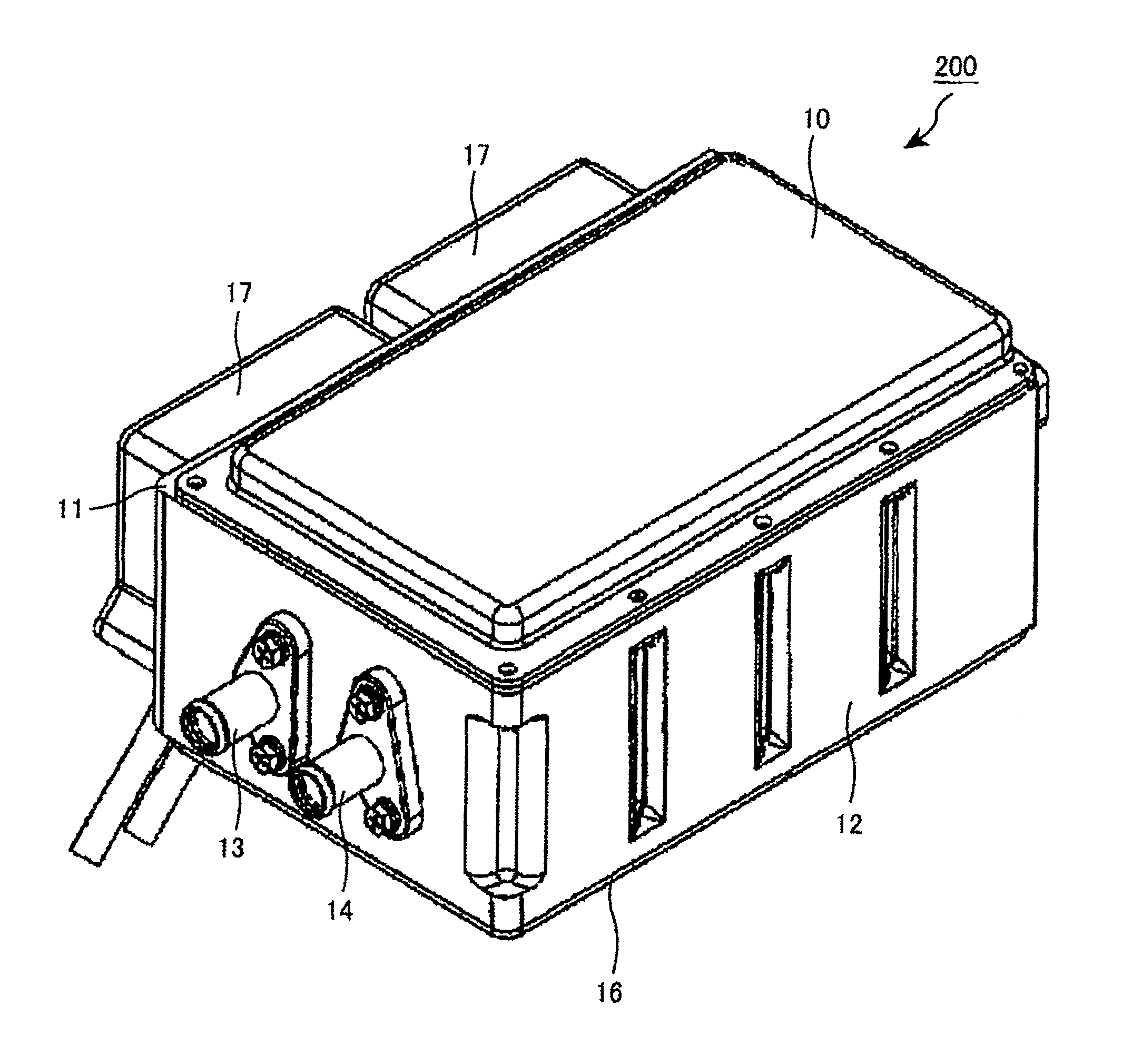
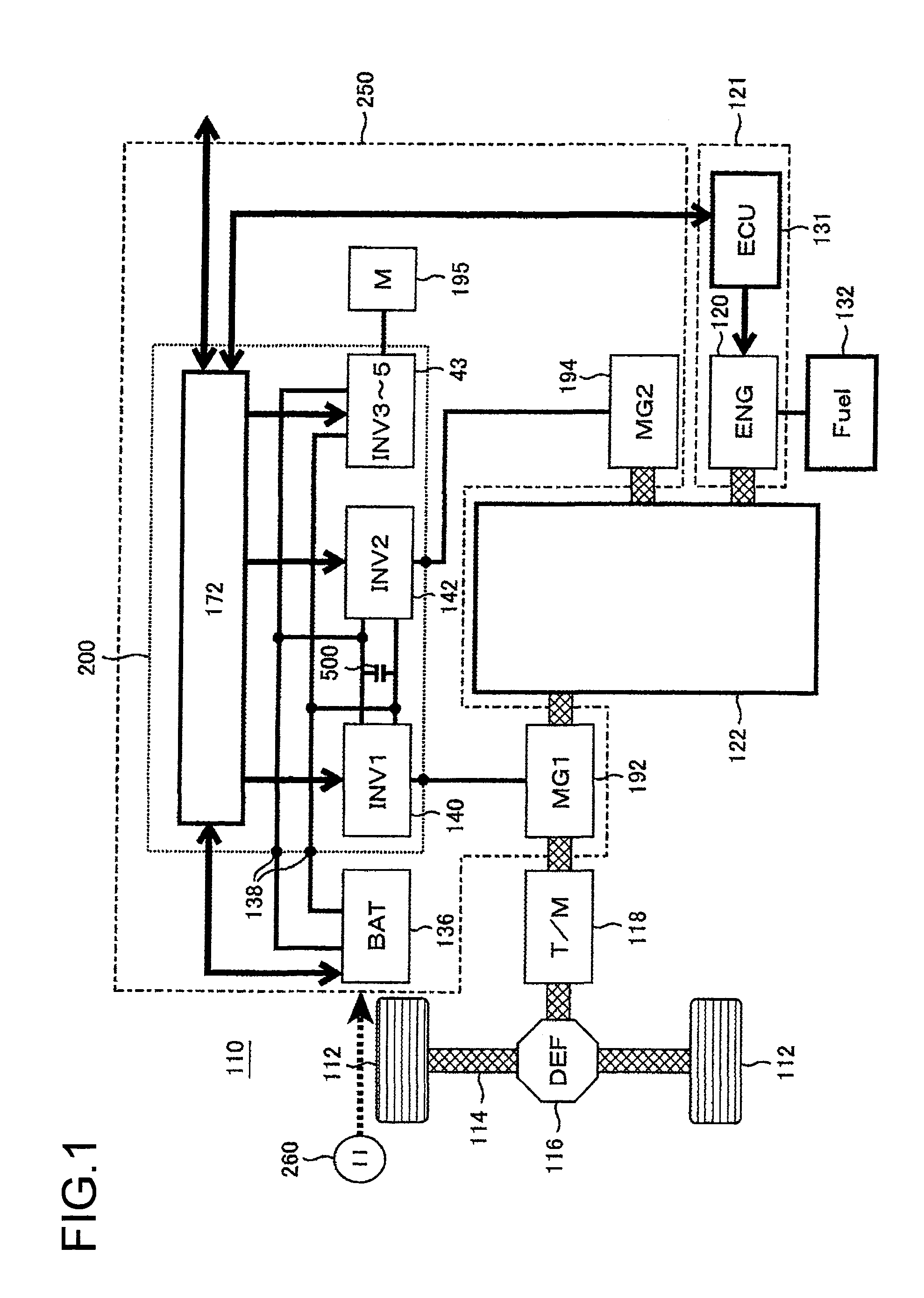
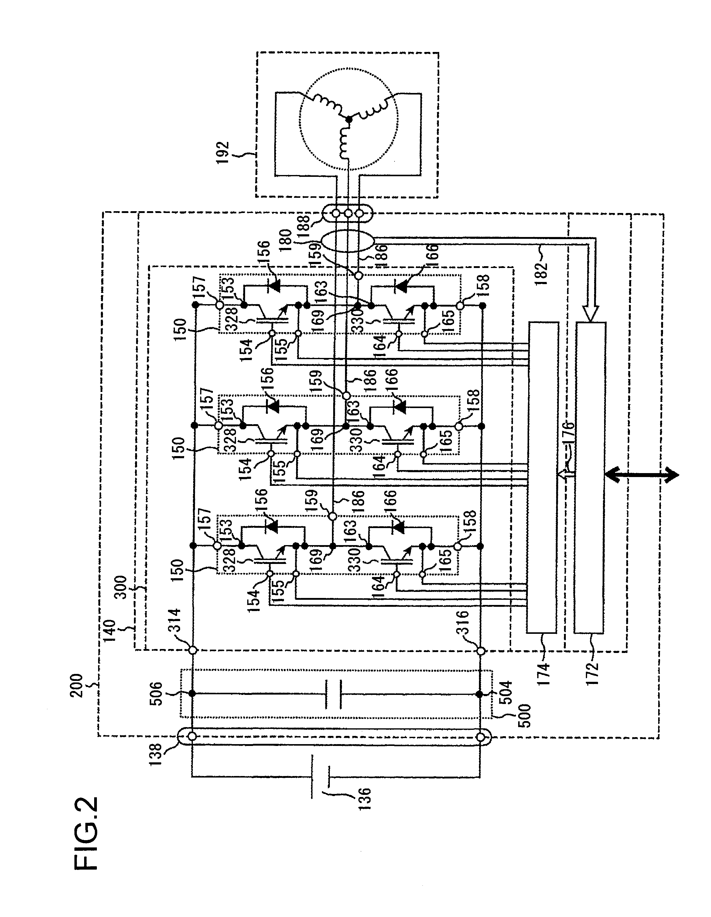
[0060]In the embodiments explained below, apart from the advantageous effect of reduction of the inductance, and the advantageous effect of being able to suppress increase of the volume, various other advantageous effects are also obtained in product manufacture. These advantageous effects will be explained below.

[0061]Apart from the problems, the operation, and the advantageous effects described in the section “Problems to be Solved by the Invention”, “Objects of the Invention” and in the section “Advantageous Effects of the Invention” as detailed above, since the embodiments of the present invention described below solve various problems directed to product improvement, and also yield various other beneficial effects, accordingly, before explaining the present invention with reference to the drawings, representative technical problems to be ameliorated and benefits to be obtained thereby, and an outline of a technique that provides the beneficial effect of solving these technical ...


PUM


Abstract

The present invention provides a vehicle power module and a power converter including a power semiconductor element (328), a plurality of connecting conductors (371U, 372U, 373U) for transmitting current to the power semiconductor element (328), and a metallic base (304) upon which the power semiconductor element (328) and the plurality of connecting conductors (371U, 372U, and 373U) are mounted; and the power semiconductor element (328) and the plurality of connecting conductors (371U, 372U, and 373U) are mounted upon the metallic base (304) so as to form a looped current path. Desirably, the power semiconductor element (328) and the plurality of connecting conductors (371U, 372U, 373U) are arranged so as to form two or more looped current paths.

Description


Claims


Application Information

Patent Timeline
Owner HITACHI ASTEMO LTD
Why Eureka
Try Eureka