Photomask design verification
- Summary
- Abstract
- Description
- Claims
- Application Information
AI Technical Summary
Problems solved by technology
Method used
Image

Examples
Embodiment Construction
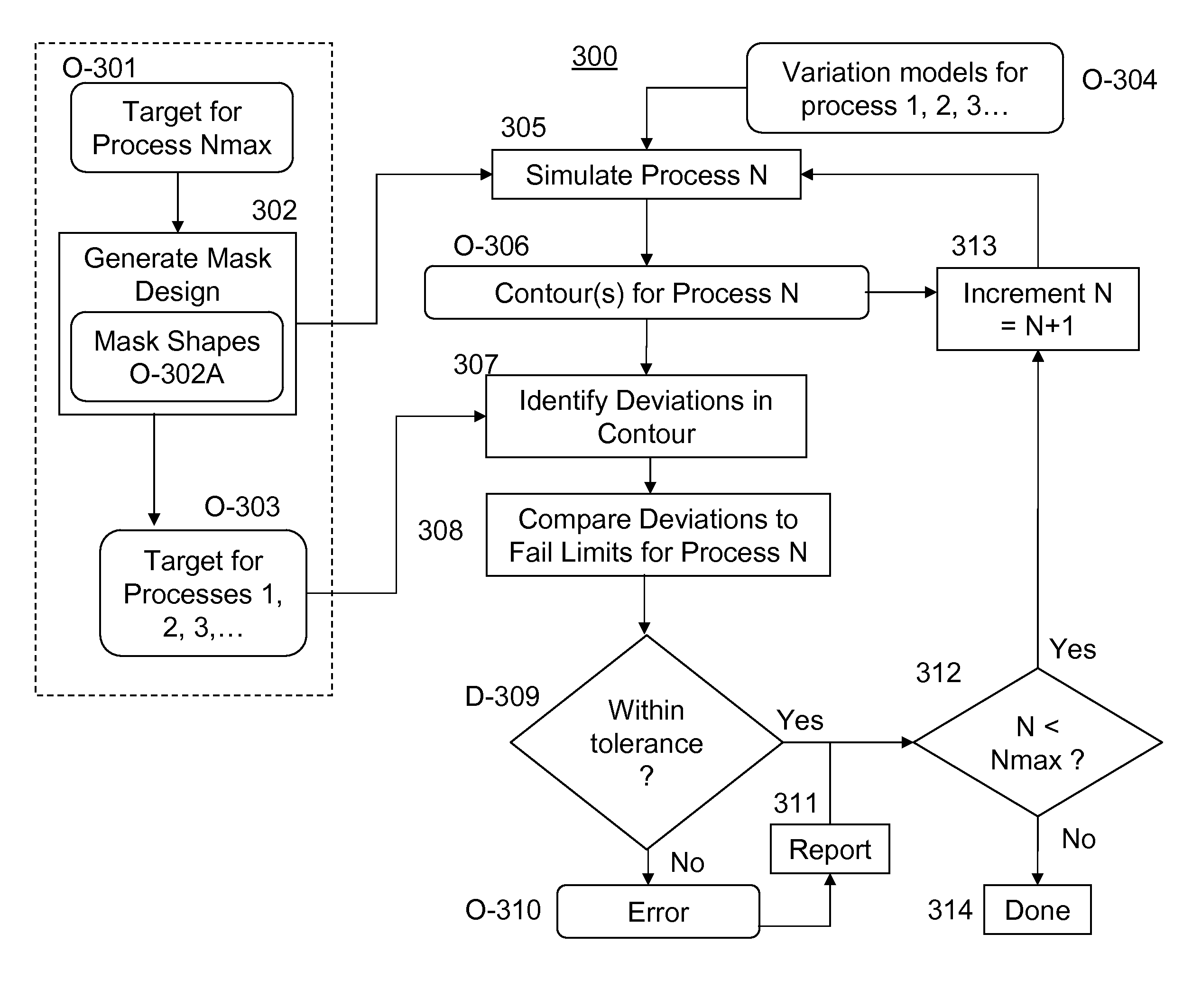
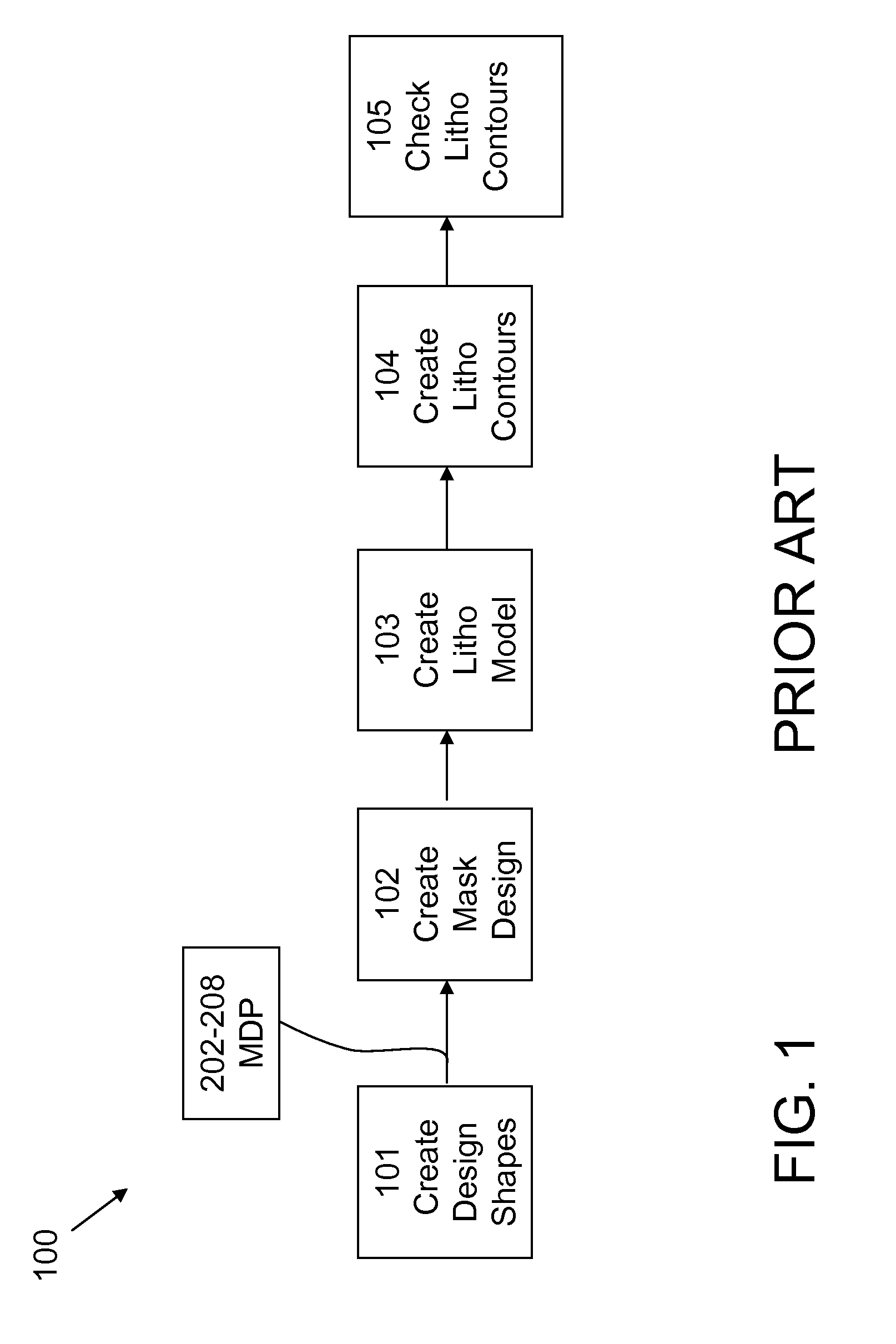
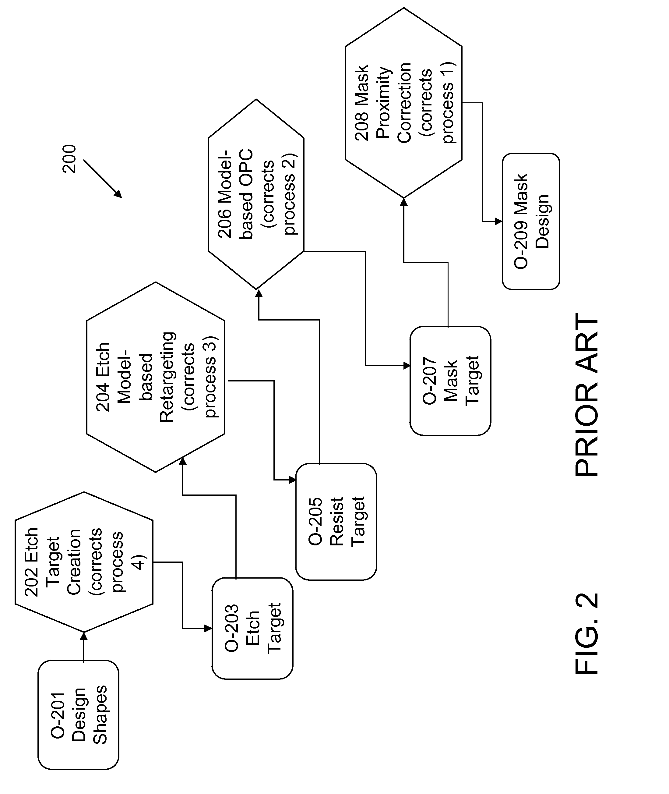
[0016]As indicated above, aspects of the invention provide solutions for verifying photomask designs. As used herein, the term “semiconductor manufacturing process” may include any of one or more steps taken in creating a semiconductor device. These processing steps may generally include, for example, designing one or more photomasks, photomask formation, lithography, etching, and verification. While portions of the disclosure specifically refer to photomask design verification, it is understood that aspects of the invention may be applied to other semiconductor manufacturing processes known in the art.
[0017]The following figures may assist in illustrating various aspects of the invention. As shown in these figures, process steps and / or specific computer system components are illustrated using rectangular boxes and / or hexagonal shapes. Objects (e.g., targets or shapes) are illustrated using boxes with rounded edges (oblong enclosures), and are labeled with the prefix “O”, while deci...
PUM
 Abstract
Description
Claims
Application Information
PatSnap Eureka turns technology decisions into work you can execute. Powered by our Innovation Knowledge Graph, it runs expert workflows across engineering, life sciences, materials and intellectual property. Get your review-ready output in minutes.


