Printed circuit board having electromagnetic bandgap structure

a printed circuit board and band gap technology, applied in the field of substrate noise reduction, can solve the problems of difficult to completely block the noise at the substrate, noise problem, and not as easy to prevent the conduction noise, and achieve the effect of reducing noise, reducing manufacturing cost, and reducing nois

Inactive Publication Date: 2011-03-17
SAMSUNG ELECTRO MECHANICS CO LTD
View PDF39 Cites 20 Cited by
  • Summary
  • Abstract
  • Description
  • Claims
  • Application Information

AI Technical Summary

Benefits of technology

[0008]The present invention provides an EMI noise reducing printed circuit board capable of getting advantages in view of spatial configuration, manufacturing cost, and power consumption, by easily reducing noises having more various frequency bands with an inductor element.

Problems solved by technology

As the operation frequencies of electronic products get higher, the electromagnetic interference (EMI) has been considered as one the chronic noise problems.
Specifically, since there has been little study on the solution to a noise generated at an edge of the substrate as the EMI problem of substrate, it is difficult to completely block the noises at the substrate.
The noise problem is caused by an EMI noise, which is the interference between electromagnetic (1M) waves generated at any one of electronic circuits, devices, parts and / or the like and other 1M waves generated at another one.
In contrast, it is not as easy to prevent the conduction noise.
Furthermore, the operation frequencies of digital electronic products get higher, causing the digital electronic products more complex, and thus it is difficult to find the solution.

Method used


Image

  • Printed circuit board having electromagnetic bandgap structure
  • Printed circuit board having electromagnetic bandgap structure
  • Printed circuit board having electromagnetic bandgap structure

Examples


Embodiment Construction

[0017]Since there can be a variety of permutations and embodiments of the present invention, certain embodiments will be illustrated and described with reference to the accompanying drawings. This, however, is by no means to restrict the present invention to certain embodiments, and shall be construed as including all permutations, equivalents and substitutes covered by the spirit and scope of the present invention.

[0018]Throughout the description of the present invention, when describing a certain technology is determined to evade the point of the present invention, the pertinent detailed description will be omitted. Terms such as “first” and “second” can be used in describing various elements, but the above elements shall not be restricted to the above terms. The above terms are used only to distinguish one element from the other.

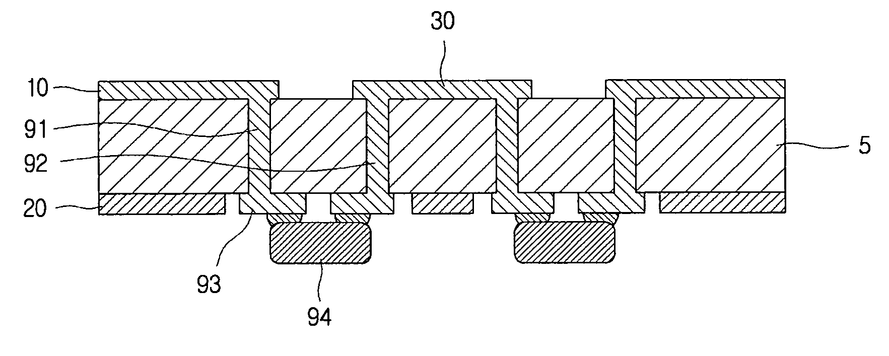
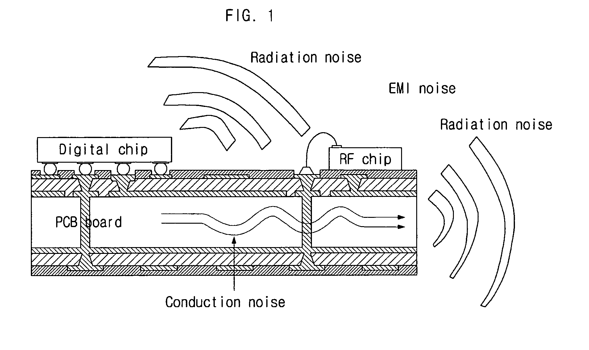
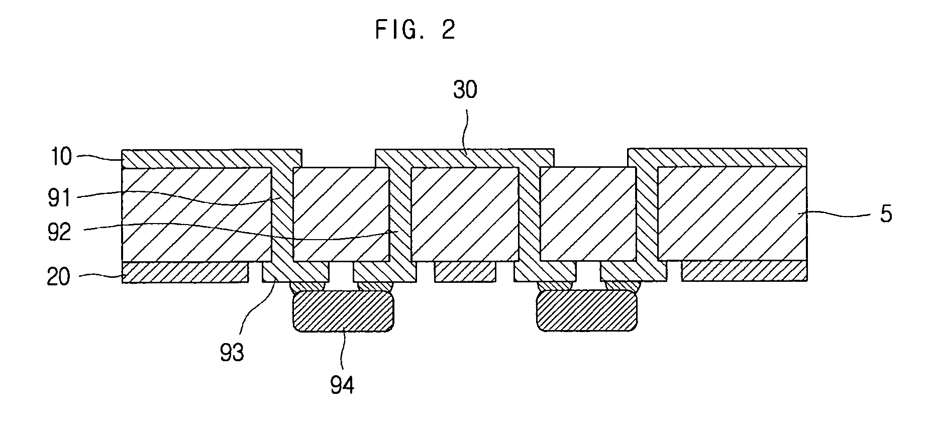
[0019]A printed circuit board in accordance with an embodiment of the present invention, as shown in FIG. 1, includes an electromagnetic bandgap structur...


PUM


Abstract

Disclosed is a printed circuit board including an electromagnetic bandgap structure. The electromagnetic bandgap structure for blocking a noise is inserted into the printed circuit board. The electromagnetic bandgap structure can include a first conductive plate; a second conductive plate arranged on a planar surface that is different from that of the first conductive plate; a third conductive plate arranged on a planar surface that is different from that of the second conductive plate; and a stitching via unit configured to connect the first conductive plate and the third conductive plate by bypassing the planar surface on which the second conductive plate is arranged and including a first inductor element.

Description

CROSS-REFERENCE TO RELATED PATENT APPLICATIONS[0001]This application claims the benefit of Korean Patent Application No. 10-2009-0087645, filed on Sep. 16, 2009, in the Korean Intellectual Property Office, the disclosure of which is incorporated herein in its entirety by reference.BACKGROUND OF THE INVENTION[0002]1. Field of the Invention[0003]The present invention relates to a substrate, more specifically to a noise reducing substrate capable of reducing a noise by using an EBG structure.[0004]2. Background Art[0005]As the operation frequencies of electronic products get higher, the electromagnetic interference (EMI) has been considered as one the chronic noise problems. Especially, the operation frequencies of the electronic products have recently been in a range of several tens MHz to several GHz, and thus it is significantly needed to solve the EMI problem. Specifically, since there has been little study on the solution to a noise generated at an edge of the substrate as the EMI...

Claims


Application Information

Patent Timeline
Patent Type & Authority Applications(United States)
IPC IPC(8): H05K9/00
CPCH05K1/0233H05K1/0236H05K2201/1003H05K2201/086H05K1/112H01L2224/16225H01L2224/48091H01L2224/48227H01L2924/00014H05K1/02
Inventor KIM, HANHAN, MI-JAPARK, DAE-HYUN
Owner SAMSUNG ELECTRO MECHANICS CO LTD
Why Eureka
Try Eureka