Substrate processing apparatus and substrate transfer method

a technology of substrate processing and processing apparatus, applied in the direction of electrical apparatus, thin material processing, article separation, etc., can solve the problems of difficult to recreate recipes with effort, the process is getting stricter, and the selection of all modules to be used becomes complicated, so as to achieve the effect of simplifying the creation of the transfer recip

Active Publication Date: 2011-03-31
TOKYO ELECTRON LTD
View PDF9 Cites 20 Cited by
  • Summary
  • Abstract
  • Description
  • Claims
  • Application Information

AI Technical Summary

Benefits of technology

[0012]In accordance with the present disclosure, if a storage container for loading, a storage container for unloading, and processing units to be used are selected, transit units to be used can be automatically selected depending on the selected storage container for loading, the selected storage container for unloading and the selected processing units. Further, a transfer route of the target substrate can be automatically calculated, and a transfer recipe can be created. Therefore, creation of a transfer recipe can be simplified and a wafer W can be transferred along a transfer route through which an optimum throughput can be obtained.

Problems solved by technology

However, recently, in such a substrate processing apparatus, a requirement for throughput of a process is getting stricter, and in order to cope with this situation, the number of processing units or transit units has increased, and, thus, it becomes complicated to select all modules to be used whenever a transfer recipe is created.
Further, since there may be a limitation in selecting the transit units depending on the selected modules, it is required to verify whether or not selection is proper at the time of creation of recipes and if not proper, it is required to recreate recipes with effort.
Meanwhile, even if selection is proper and a transfer is available, it is difficult to know whether or not an optimum transit unit has been selected in view of throughput.

Method used


Image

  • Substrate processing apparatus and substrate transfer method
  • Substrate processing apparatus and substrate transfer method
  • Substrate processing apparatus and substrate transfer method

Examples


Embodiment Construction

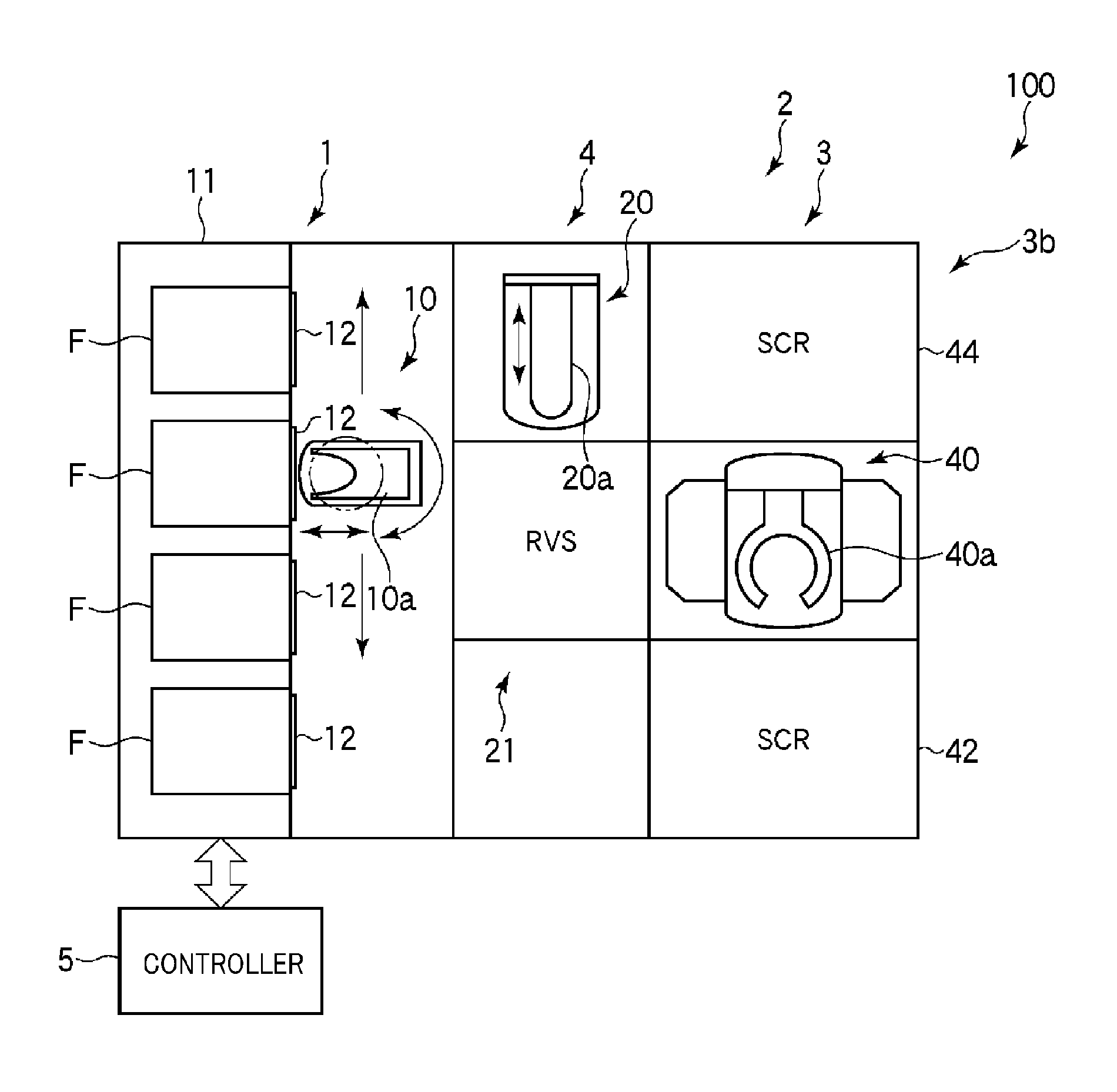
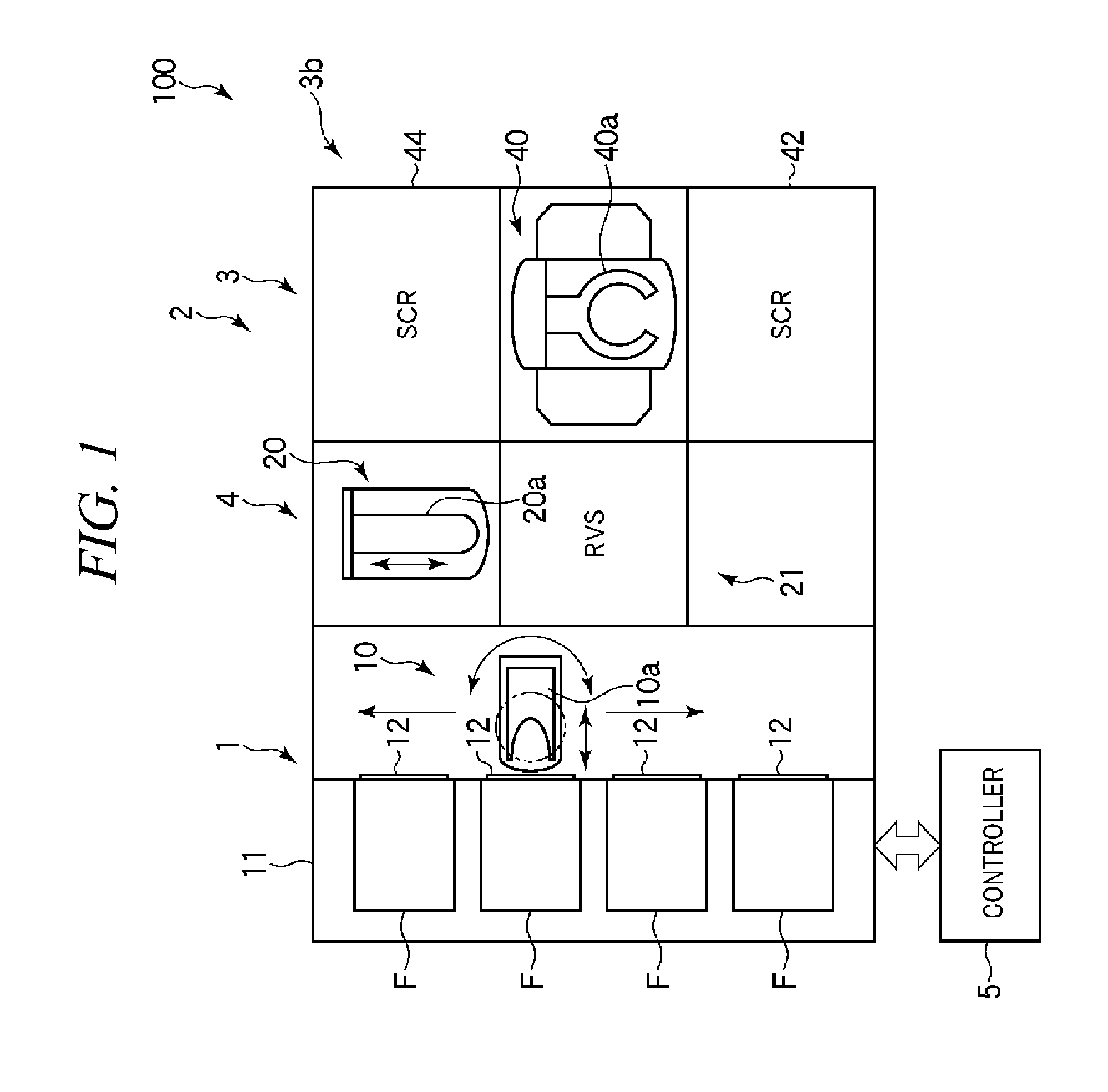
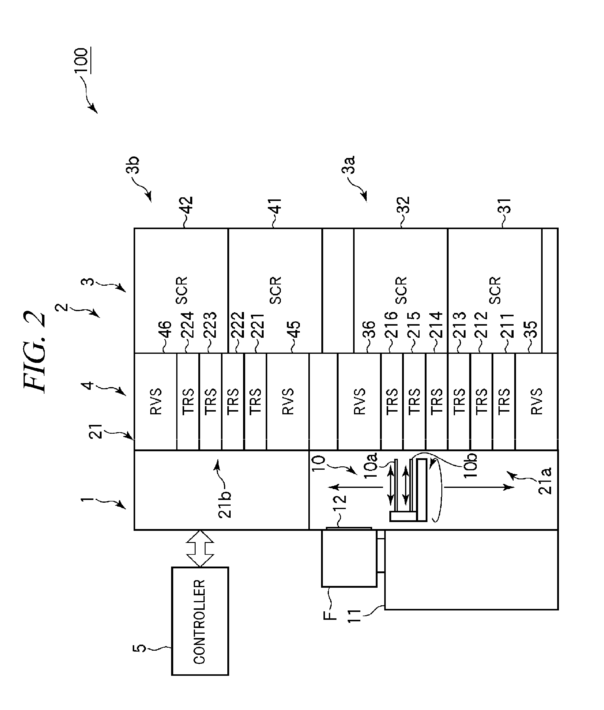
[0026]Hereinafter, embodiments of the present disclosure will be explained in detail with reference to accompanying drawings. In the present embodiment, there will be explained a substrate processing apparatus configured as a cleaning apparatus in which a scrub cleaning process is performed onto a front surface and a rear surface of a semiconductor wafer (hereinafter, simply referred to as “wafer”) serving as a target substrate. Here, the front surface of the wafer is a device forming surface and the rear surface is the opposite surface thereof.

[0027]FIG. 1 is a plane view of a schematic configuration of a substrate processing apparatus in accordance with the present embodiment, FIG. 2 is a longitudinal cross sectional side view thereof, FIG. 3 shows the inside of a processing block of the substrate processing apparatus of FIG. 1, FIG. 4 shows the processing block when viewed from the opposite side of a loading / unloading block, and FIG. 5 shows a stacked tower and a delivery transfe...


PUM


Abstract

A substrate processing apparatus includes a loading/unloading unit including a mounting table on which a storage container accommodating a target substrate is mounted; a processing unit set including a plurality of processing units that perform a process on the target substrate; a plurality of transit units that transit the target substrate between the loading/unloading unit and the processing unit set; a selection unit that receives input for selecting a storage container for loading, a storage container for unloading, and a processing unit to be used for processing the target substrate; and a transfer recipe creating unit that automatically selects a transit unit to be used among the plurality of transit units based on the storage container for loading, the storage container for unloading, and the processing unit selected through the selection unit, automatically generates a transfer route of the target substrate, and creates a transfer recipe.

Description

CROSS-REFERENCE TO RELATED APPLICATION[0001]This application claims the benefit of Japanese Patent Application No. 2009-226458 filed on Sep. 30, 2009 and Japanese Patent Application No. 2010-186263 filed on Aug. 23, 2010, the entire disclosures of which are incorporated herein by reference.FIELD OF THE INVENTION[0002]The present disclosure relates to a substrate processing apparatus which transfers a substrate to one of a plurality of processing units from a storage container accommodating the substrate and performs a process onto the substrate, and a substrate transfer method of the substrate processing apparatus.BACKGROUND OF THE INVENTION[0003]In a manufacturing process of a semiconductor device or in a manufacturing process of a flat panel display (FPD), there has been performed a cleaning process for removing particles or contaminations or a resist coating and developing process to a target substrate such as a semiconductor wafer or a glass substrate.[0004]In a substrate proces...

Claims


Application Information

Patent Timeline
Patent Type & Authority Applications(United States)
IPC IPC(8): H01L21/677
CPCH01L21/67184H01L21/67778H01L21/67253H01L21/67225H01L21/67769Y10S414/137
Inventor ITOU, KOUICHI
Owner TOKYO ELECTRON LTD
Why Eureka
Try Eureka