Unlock instant, AI-driven research and patent intelligence for your innovation.

Unified Addressing and Instructions for Accessing Parallel Memory Spaces

a parallel memory space and instruction technology, applied in the field of memory systems, can solve the problems of not knowing compilers cannot determine which memory access instruction to insert, and insufficient dynamic case insertion of sequence of several instructions,

Active Publication Date: 2011-03-31
NVIDIA CORP
View PDF6 Cites 19 Cited by
  • Summary
  • Abstract
  • Description
  • Claims
  • Application Information

AI Technical Summary

Benefits of technology

[0008]One embodiment of the present invention sets forth a technique that enables a program to use a common load or store instruction to access distinct parallel memory spaces having different scopes. A unified memory space address is converted into an address that accesses only one of the parallel memory spaces. One advantage of the unified memory space address conversion is that a single type of load or store instruction may be used that specifies the unified memory space address instead of using a different type of load or store instruction to access each of the distinct parallel memory spaces.

Problems solved by technology

When a C / C++ function is compiled separately from the calling code, the compiler does not know which memory space a pointer passed as a function argument references, and therefore does not know which memory access instruction to insert.
Similarly, when a function is called from multiple calling points with pointer arguments to different memory spaces, or via a pointer to the function, the compiler cannot determine which memory access instruction to insert.
Inserting sequence of several instructions works for some static compile-time cases, but is not sufficient for dynamic cases, such as multiple calls to a library function via a function pointer, or separately-compiled functions.

Method used


Image

  • Unified Addressing and Instructions for Accessing Parallel Memory Spaces
  • Unified Addressing and Instructions for Accessing Parallel Memory Spaces
  • Unified Addressing and Instructions for Accessing Parallel Memory Spaces

Examples


Embodiment Construction

[0021]In the following description, numerous specific details are set forth to provide a more thorough understanding of the present invention. However, it will be apparent to one of skill in the art that the present invention may be practiced without one or more of these specific details. In other instances, well-known features have not been described in order to avoid obscuring the present invention.

System Overview

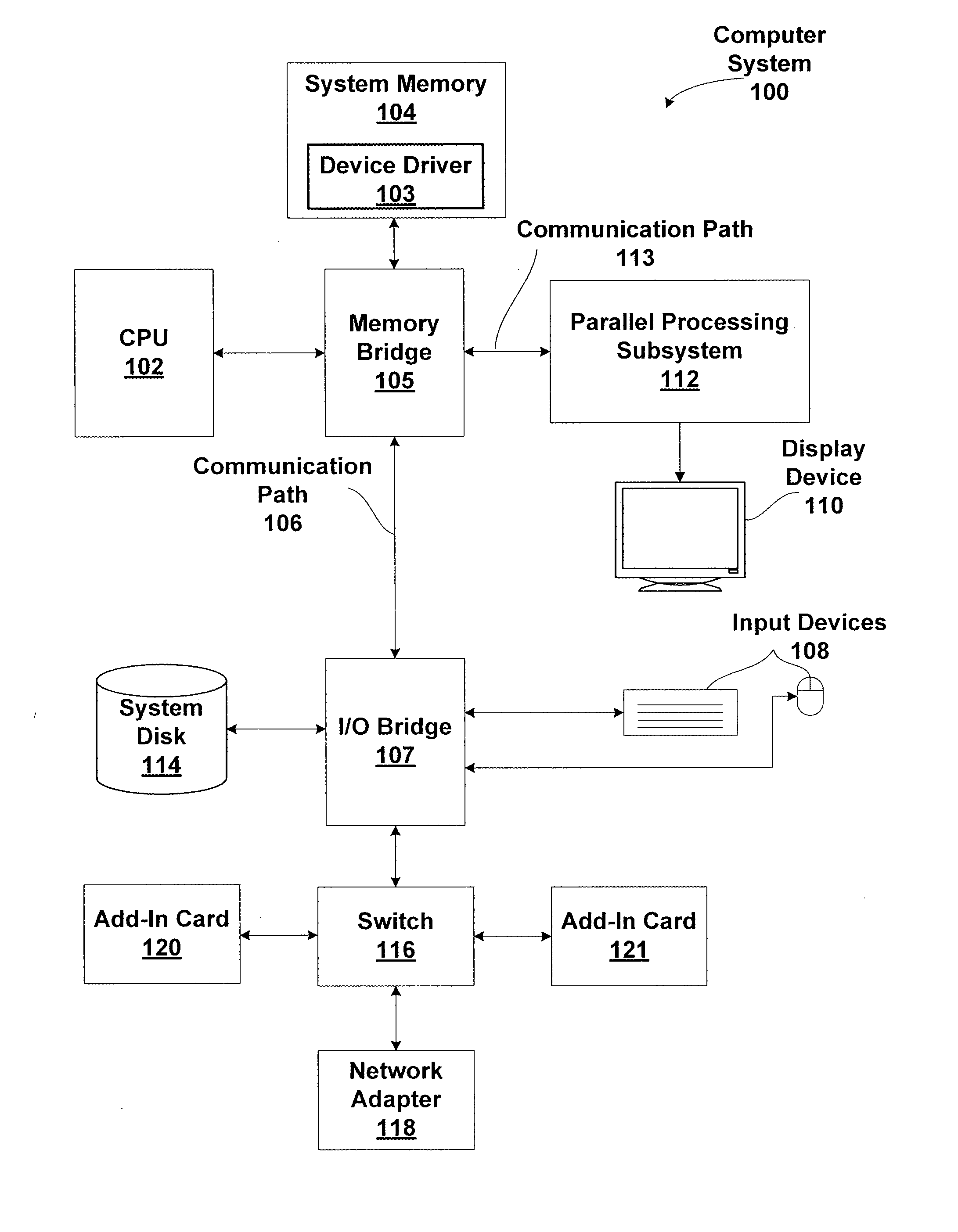
[0022]FIG. 1 is a block diagram illustrating a computer system 100 configured to implement one or more aspects of the present invention. Computer system 100 includes a central processing unit (CPU) 102 and a system memory 104 communicating via an interconnection path that may include a memory bridge 105. Memory bridge 105, which may be, e.g., a Northbridge chip, is connected via a bus or other communication path 106 (e.g., a HyperTransport link) to an I / O (input / output) bridge 107. I / O bridge 107, which may be, e.g., a Southbridge chip, receives user input from one or mor...


PUM


Abstract

One embodiment of the present invention sets forth a technique for unifying the addressing of multiple distinct parallel memory spaces into a single address space for a thread. A unified memory space address is converted into an address that accesses one of the parallel memory spaces for that thread. A single type of load or store instruction may be used that specifies the unified memory space address for a thread instead of using a different type of load or store instruction to access each of the distinct parallel memory spaces.

Description

BACKGROUND OF THE INVENTION[0001]1. Field of the Invention[0002]The present invention generally relates to memory systems and more specifically to unifying the addressing of multiple distinct memory spaces into a single address space.[0003]2. Description of the Related Art[0004]Performance requirements are constantly increasing in data processing systems. Multiple processing units may be configured to operate in parallel by the execution of multiple parallel threads. For some applications the multiple parallel threads execute independently. For other applications, the multiple parallel threads share some data. For example, a first thread may compute an input that is used by one or more other threads. Finally, the threads may be organized in groups, where data is shared within each group, but not between groups.[0005]Multithreaded parallel programs written using a programming model such as the CUDA™ C (general purpose parallel computing architecture) and PTX™ (a low-level parallel th...

Claims


Application Information

Patent Timeline
IPC IPC(8): G06F12/10
CPCG06F12/109G06F13/404G06F2212/656G06F2212/302G06F12/0284G06F12/1054G06F12/1036
Inventor NICKOLLS, JOHN R.COON, BRETT W.BUCK, IAN A.GLANVILLE, ROBERT STEVEN
Owner NVIDIA CORP
Features
  • R&D
  • Intellectual Property
  • Life Sciences
  • Materials
  • Tech Scout
  • Unparalleled Data Quality
  • Higher Quality Content
  • 60% Fewer Hallucinations
Learn More