Semiconductor device

a technology of semiconductor devices and semiconductors, applied in the direction of semiconductor devices, basic electric elements, electrical equipment, etc., can solve the problems of difficult electric field concentration and inability to increase the electric strength of semiconductor devices so much, and achieve the effect of high electric strength

Active Publication Date: 2011-04-07
TOYOTA JIDOSHA KK
View PDF55 Cites 10 Cited by
  • Summary
  • Abstract
  • Description
  • Claims
  • Application Information

AI Technical Summary

Benefits of technology

[0023]The semiconductor devices disclosed in this specification has high electric strength, because the electric field concentration does not occur easily in the semiconductor layer.

Problems solved by technology

Therefore, an electric strength of the semiconductor device can not be increased so much merely by the peripheral electrode.
As just described, in this semiconductor device, because the extension of the depleted layer is suppressed at the two points, the concentration of the electric field does not easy occur compared with the semiconductor device not having the intermediate electrode.

Method used


Image

  • Semiconductor device
  • Semiconductor device
  • Semiconductor device

Examples


first embodiment

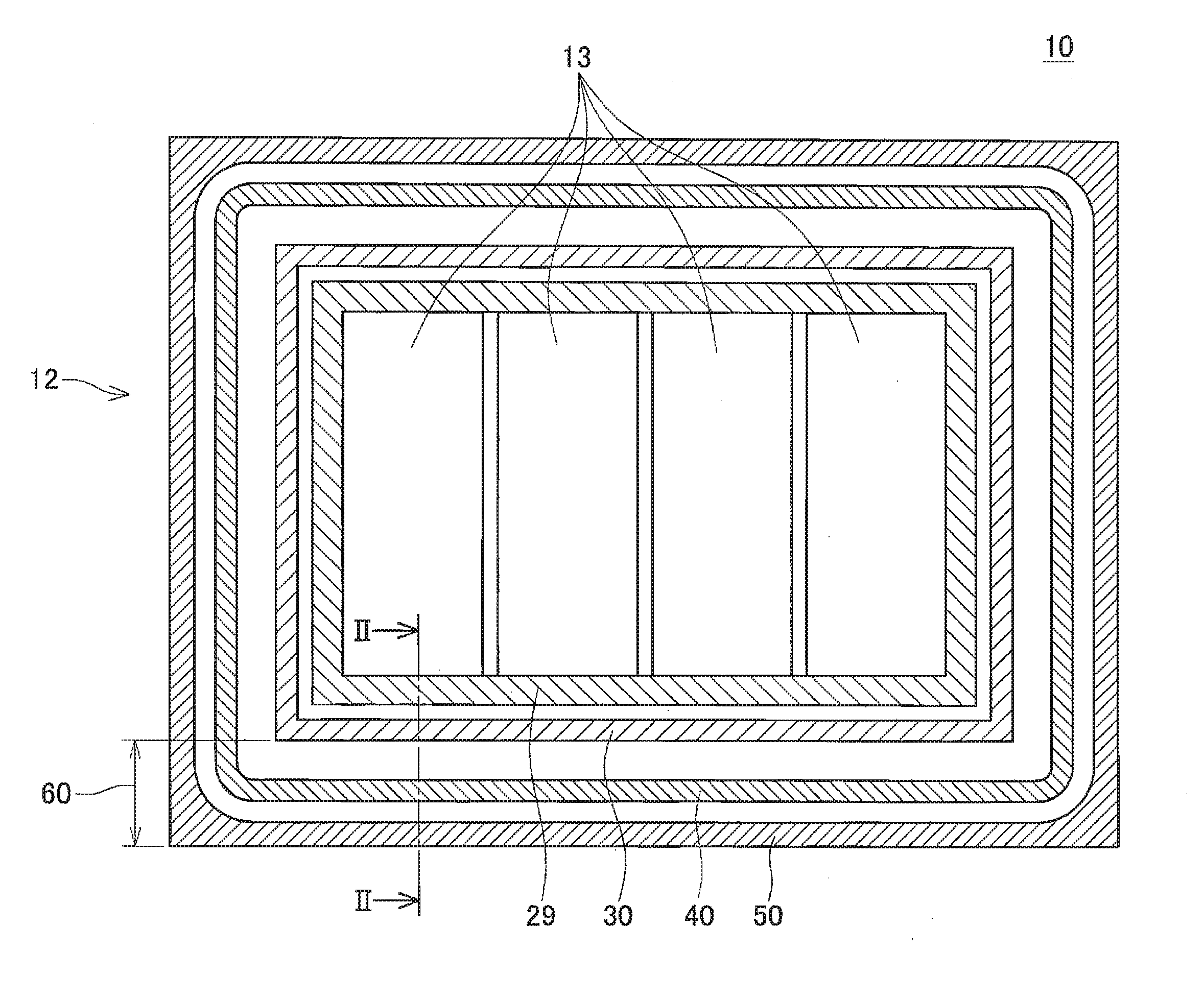
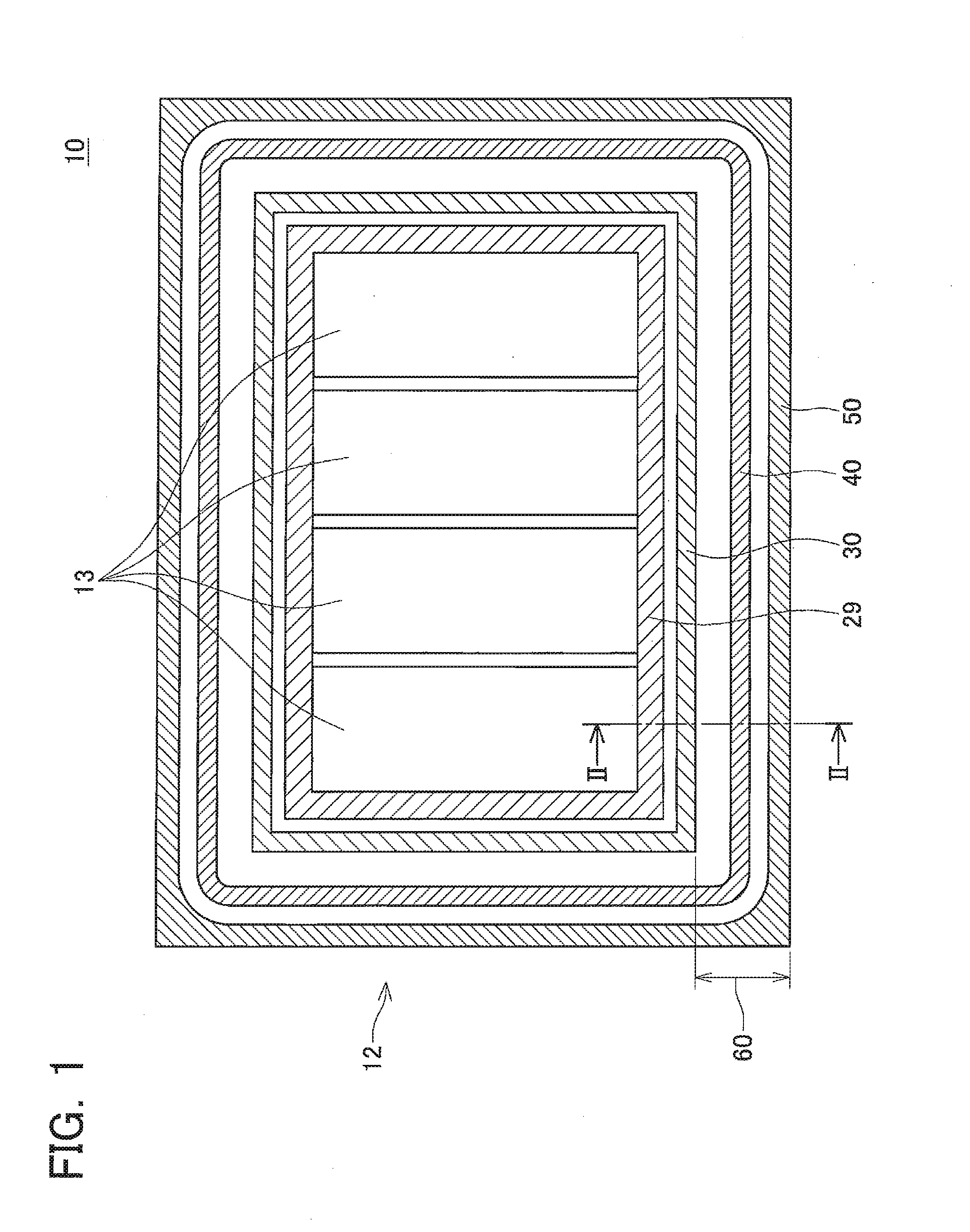
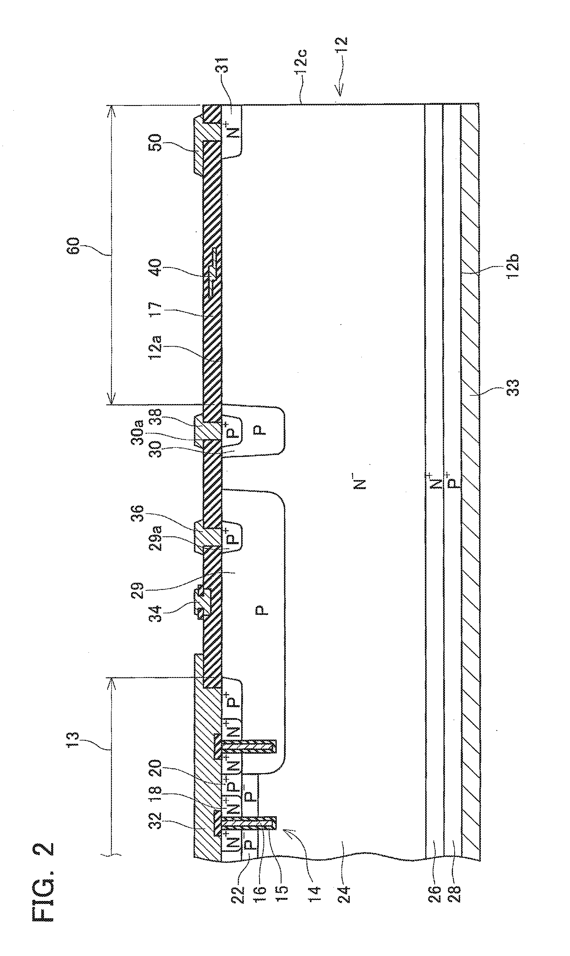
[0040]FIG. 1 shows a top view of an IGBT 10 (a semiconductor device) of the first embodiment. The IGBT 10 is configured by a semiconductor substrate 12, electrodes, insulating films and so on which are formed on an upper surface 12a and a lower surface 12b of the semiconductor substrate 12. Note that the electrodes and the insulating films formed on the semiconductor substrate 12 with exceptions of an intermediate electrode 40 and a peripheral electrode 50, are not indicated in FIG. 1. As shown in FIG. 1, four semiconductor element regions 13 are formed in the semiconductor substrate 12. Within the semiconductor element regions 13, IGBT structures are formed. An FLR 29, an FLR 30 and a peripheral termination region 60 are formed in the semiconductor substrate 12 to surround the four semiconductor element regions 13. On the peripheral termination region 60, the intermediate electrode 40 and the peripheral electrode 50 are formed. Note that the FLR 29, the FLR 30, the intermediate ele...

second embodiment

[0064]Next, an IGBT 110 of the second embodiment is described. Note that portions of the IGBT 110, which have the same function as the portions of the IGBT 10 of the first embodiment, are given the same reference numbers as the first embodiment. Furthermore, the IGBT 110 of the second embodiment is different only in the intermediate electrode from the IGBT 10 of the first embodiment. Therefore, the IGBT 110 of the second embodiment is described in relation to only the intermediate electrode. FIG. 10 shows an enlarged cross-sectional view of the peripheral termination region 60 of the IGBT 110 of the second embodiment. As shown in FIG. 10, in the IGBT 110 of the second embodiment, two intermediate electrodes 41a, 41b are formed within the interlayer dielectric film 17 within the peripheral termination region 60. FIG. 11 shows a top view of the semiconductor substrate 12 of the IGBT 110 of the second embodiment. As shown in FIG. 11, the intermediate electrode 41a surrounds the four se...


PUM


Abstract

This specification discloses a semiconductor device having higher electric strength.The semiconductor device disclosed in this specification has a semiconductor element region, a peripheral termination region, a peripheral electrode, an insulating film, and an intermediate electrode. A semiconductor element is formed within the semiconductor element region. The peripheral termination region is formed around the semiconductor element region and formed of a single conductive type semiconductor. The semiconductor element region and the peripheral termination region are exposed at one surface of a semiconductor substrate. The peripheral electrode is formed on a surface of the peripheral termination region and along a circumference of the semiconductor substrate. The insulating film is formed on the surface of the peripheral termination region and between the semiconductor element region and the peripheral electrode. The intermediate electrode is formed on the insulating film. A thickness of the insulating film under the intermediate electrode is larger at a side of the peripheral electrode than at a side of the semiconductor element region.

Description

TECHNICAL FIELD[0001]The present invention relates to a semiconductor device. Especially, the present invention relates to a semiconductor device in which a termination structure is formed between a circumference of a semiconductor substrate and a semiconductor element region.BACKGROUND ART[0002]In Japanese Published Patent Application No. 2003-133555, a semiconductor device in which a peripheral electrode is formed along a circumference of an upper surface of a semiconductor substrate is disclosed. The peripheral electrode is electrically connected with a semiconductor layer. Because the peripheral electrode is formed, when the semiconductor device is not conducting, a depleted layer extending from a semiconductor element region (the semiconductor element region is a region in which a semiconductor element is formed) is terminated in the semiconductor layer under the peripheral electrode. Therefore, the depleted layer is prevented from reaching the circumference of the semiconducto...

Claims


Application Information

Patent Timeline
Patent Type & Authority Applications(United States)
IPC IPC(8): H01L29/06
CPCH01L29/402H01L29/404H01L29/7395H01L29/42316H01L29/41725
Inventor SENOO, MASARU
Owner TOYOTA JIDOSHA KK
Why Eureka
Try Eureka