Semiconductor component and method for producing the same

A technology of semiconductors and components, applied in the field of manufacturing vertical semiconductor components, can solve problems such as need, expensive technology, difficult to adjust metal masks, etc.

Active Publication Date: 2006-05-10
INFINEON TECH AG
View PDF1 Cites 9 Cited by
  • Summary
  • Abstract
  • Description
  • Claims
  • Application Information

AI Technical Summary

Problems solved by technology

The disadvantage of this known method is that it requires expensive technology with metal masks that are difficult to adjust
In addition, it should ...

Method used


Image

  • Semiconductor component and method for producing the same
  • Semiconductor component and method for producing the same
  • Semiconductor component and method for producing the same

Examples


Embodiment Construction

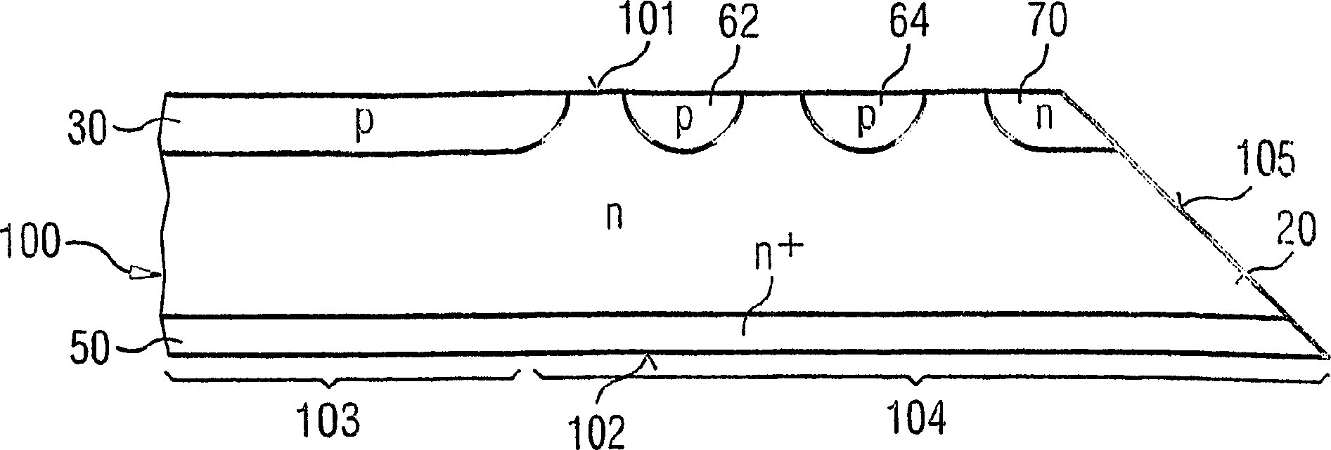
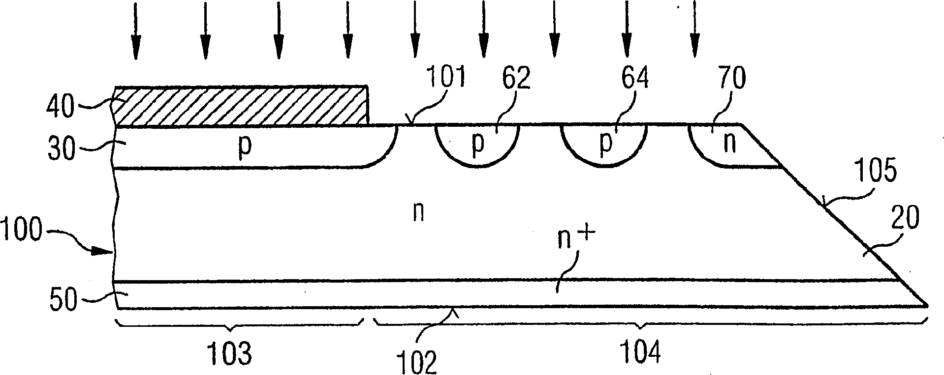
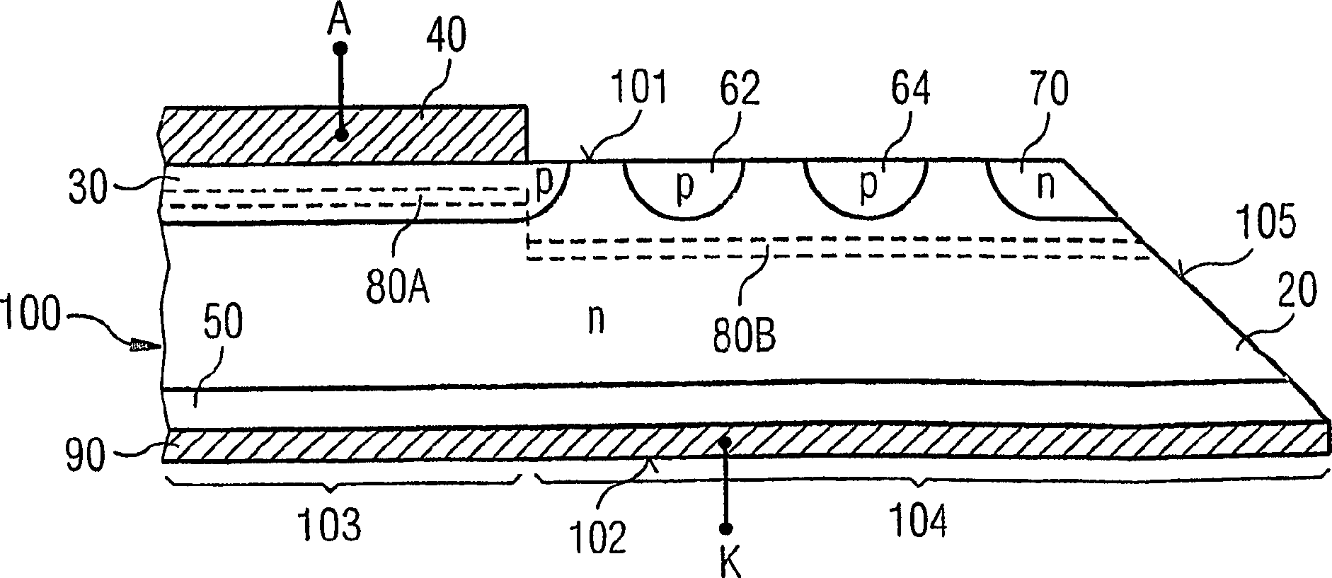
[0026] Below with the help of the fabrication of vertical power diodes Figure 1-3 A method for manufacturing a semiconductor element according to the present invention will be described. The method involves preparing figure 1 The semiconductor body 100 is partially shown in cross-section. The semiconductor body 100 has a front side 101 , a rear side 102 and, in the exemplary embodiment, a chamfered edge 105 . The semiconductor body comprises an inner region 103 spaced apart from an edge 105 and an edge region 104 arranged between the inner region 103 and the edge. The illustrated semiconductor body 100 has an n background doping, the semiconductor region having this background doping being referred to below as the first semiconductor region 20 . In the first semiconductor region 20, a p-doped second semiconductor region 30 is introduced in the inner region 103 below the front side 101, so that a p-doped second semiconductor region 30 is formed between the second semiconduc...


PUM


Abstract

The invention relates to a method for producing a semiconductor component, the method comprising the method steps of irradiating the front side (101) of a semiconductor body (100) with energetic particles using a connecting electrode (40) as a mask in order to Recombination centers (80A, 80B) for recombining charge carriers of the first and second conductivity type are generated in the semiconductor body (100).

Description

technical field [0001] The invention relates to a method for producing a vertical semiconductor component having a semiconductor body with an inner region, at least one pn junction present in the inner region and an edge arranged between the inner region and the edge area. Current flows through such components when a suitable voltage is applied in the vertical direction, ie perpendicular to the front and back sides of the semiconductor body. Such a vertical semiconductor component having an inner region and an edge region adjoining the inner region is described, for example, in US Pat. No. 6,351,024 B1, wherein the inner region has a pn junction. Background technique [0002] When switching off such semiconductor components, that is to say when applying a voltage which breaks the pn junction, the edge region is of importance, as will be briefly explained below. In the case of electrically polarized pn junctions, the edge region is likewise filled with charge carriers, ie e...

Claims


Application Information

Patent Timeline
IPC IPC(8): H01L29/32H01L29/861
CPCH01L21/263H01L29/0615H01L29/0619H01L29/0638H01L29/0661H01L29/0692H01L29/32H01L29/8611
Inventor R·巴特梅斯H·-J·舒尔泽
Owner INFINEON TECH AG
Why Eureka
Try Eureka