
Semiconductor Integrated Circuit Device

a technology of integrated circuits and semiconductors, applied in the field of technology, can solve problems such as conversion errors and the number of external terminals, and achieve the effect of high conversion precision and reduced conversion errors in a/d converters

Active Publication Date: 2011-04-14
RENESAS ELECTRONICS CORP
View PDF4 Cites 4 Cited by
  • Summary
  • Abstract
  • Description
  • Claims
  • Application Information

AI Technical Summary

Benefits of technology

[0011]An object of the present invention is to provide a technique capable of performing A / D conversion at high precision while largely reducing the number of external terminals used for an A / D converter.
[0026](1) Since the impedance optimum for sampling and the impedance optimum for the successive approximation can be set, the noise cancelling effect can be obtained maximally, and the influence of noise and the like can be largely reduced.
[0027](2) By the effect (1), a conversion error in the A / D converter can be largely reduced, and high conversion precision can be realized.

Problems solved by technology

However, the inventors have found out that the technique of decreasing the number of external terminals in the semiconductor integrated circuit device having the plurality of A / D converters has the following problem.
When noise occurs in the power supply terminals and reference terminals at the time of comparison by a comparator after completion of sampling, a conversion error is caused.

Method used


Image

  • Semiconductor Integrated Circuit Device
  • Semiconductor Integrated Circuit Device
  • Semiconductor Integrated Circuit Device

Examples


first embodiment

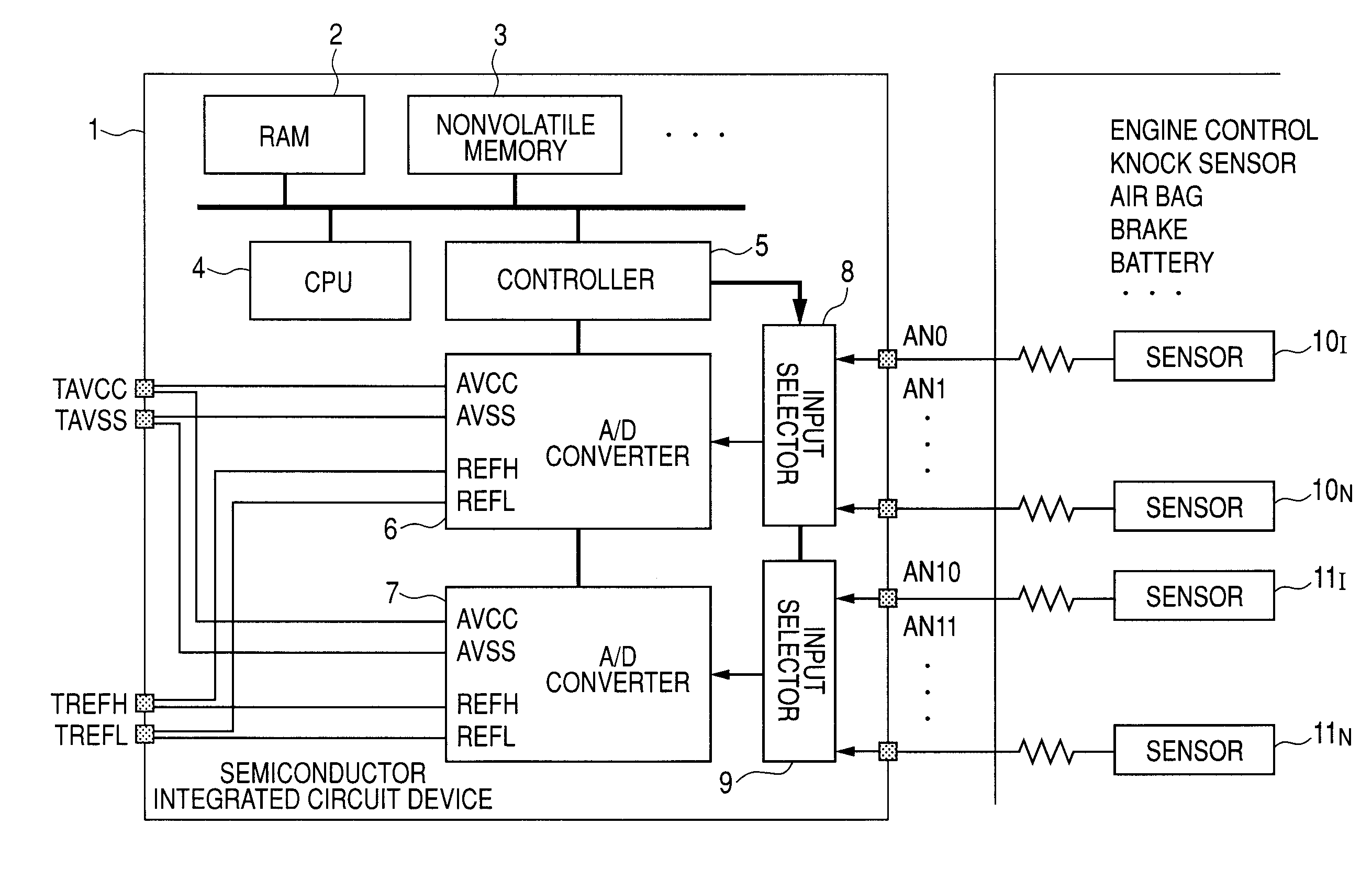
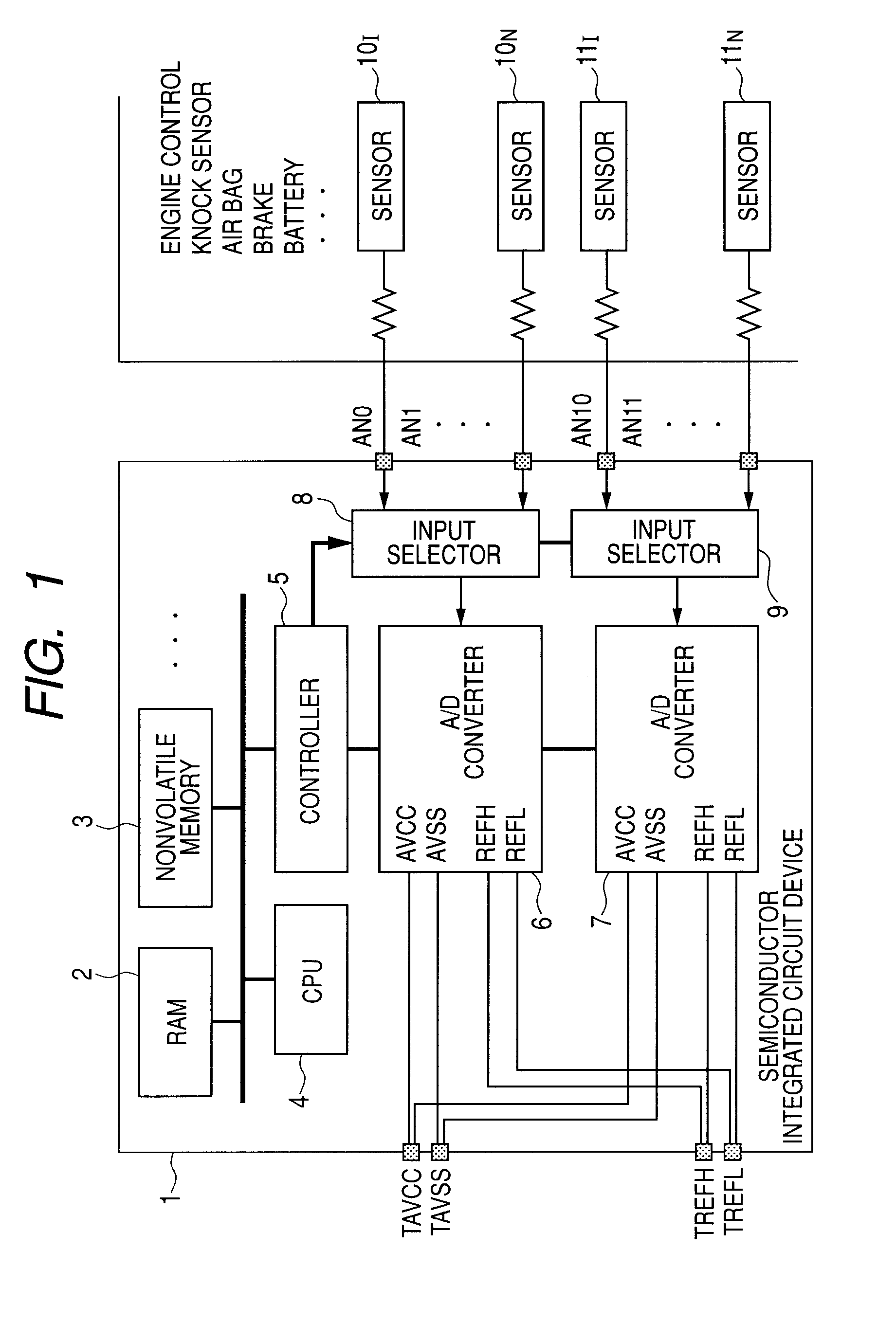
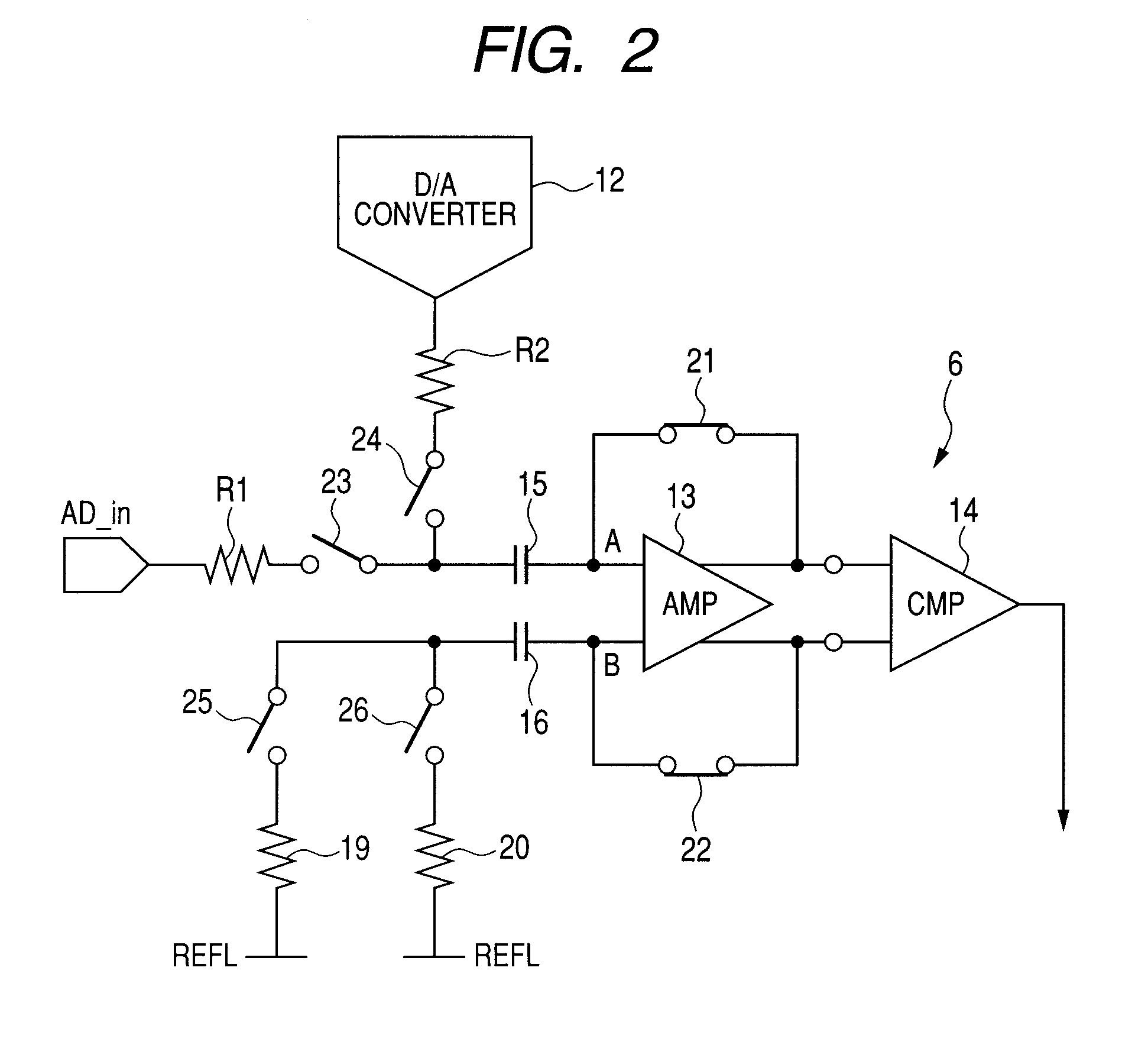
[0043]FIG. 1 is a block diagram showing an example of a semiconductor integrated circuit device according to a first embodiment of the invention. FIG. 2 is an explanatory diagram showing an example of an A / D converter provided for the semiconductor integrated circuit device of FIG. 1. FIG. 3 is an explanatory diagram showing an example of a prior art A / D converter examined by the inventors of the present invention. FIG. 4 is a timing chart showing an example of operation in the A / D converter of FIG. 3. FIG. 5 is a timing chart showing an example of operation in the A / D converter of FIG. 2.

[0044]In the first embodiment, a semiconductor integrated circuit device 1 is mounted on, for example, a vehicle and performs controls on various systems such as engine control, air-bag control, and air-conditioner control. The semiconductor integrated circuit device 1 has, as shown in FIG. 1, a RAM 2, a nonvolatile memory 3, a CPU 4, a controller 5, A / D converters 6 and 7, and input selectors 8 an...

second embodiment

[0091]FIG. 6 is an explanatory diagram showing an example of an A / D converter in a second embodiment of the invention, and FIG. 7 is an explanatory diagram showing an example of layout in a part of the A / D converter of FIG. 6.

[0092]The second embodiment relates to the case of mounting a capacitive D / A converter 12a of a charge re-distribution type on the A / D converter 6 (7) in the first embodiment, and the capacitance of a sampling capacitive D / A converter is commonly used.

[0093]As shown in FIG. 6, the A / D converter 6 has the capacitive D / A converter 12a, the amplifier 13, the comparator 14, the reference capacitance element 16, the resistors 19 and 20, resistors 29 and 30, and the switches 21, 22, 25, and 26. Although the A / D converter 6 is shown in FIG. 6, the A / D converter 7 also has a configuration similar to that of the A / D converter 6.

[0094]Since the connection configuration of the amplifier 13, the comparator 14, the reference capacitance element 16, the resistors 19 and 20, ...

third embodiment

[0123]FIG. 9 is an explanatory diagram showing an example of the configuration of an A / D converter according to a third embodiment of the invention, and FIG. 10 is a timing chart showing an example of the operation in the A / D converter 6 of FIG. 9.

[0124]In the third embodiment, as shown in FIG. 9, the A / D converter 6 includes the D / A converter 12, the amplifier 13, the comparator 14, the capacitance elements 15 and 16, the resistors 19 and 20, and the switches 21 to 26.

[0125]The configuration is similar to that shown in FIG. 2 of the first embodiment, and the difference is coupling of the switches 25 and 26 and the resistors 19 and 20. In this case, to the one coupling part of the reference capacitance element 16, one of coupling parts of the switch 25 and one of coupling parts of the resistor 19 are coupled.

[0126]To the other coupling part of the switch 25 and the other coupling part of the resistor 19, one of coupling parts of the switch 26 and one of coupling parts of the resisto...


PUM


Abstract

A high-precision A / D conversion is realized while the number of external terminals used for an A / D converter is reduced. At the time of sampling, first to fifth switches are turned on and a sixth switch is turned off. Since a first resistor is set to a resistance value optimum for sampling, an impedance in the direction from a node A to the left side and an impedance in the direction from a node B to the left side almost match, and a large noise-cancelling effect is obtained. At the time of successive approximation, the first, second, third, and fifth switches are turned off and the fourth and sixth switches are turned on. Since a second resistor is set to a resistance value optimum for the successive approximation, the impedance in the direction from the node A to the left side and the impedance in the direction from the node B to the left side almost match, and a large noise-cancelling effect is obtained also at the time of successive approximation.

Description

CROSS-REFERENCE TO RELATED APPLICATIONS[0001]The disclosure of Japanese Patent Application No. 2009-234717 filed on Oct. 9, 2009 including the specification, drawings and abstract is incorporated herein by reference in its entirety.BACKGROUND OF THE INVENTION[0002]The present invention relates to a technique for improving precision of conversion of an A / D (Analog / Digital) converter and, more particularly, to a technique effective to reduce a conversion error in a semiconductor integrated circuit device on which a plurality of A / D converters are mounted.[0003]A semiconductor integrated circuit device on which an A / D converter is mounted is widely used. For example, in a semiconductor integrated circuit device used for controlling a car or the like, there is a tendency that the number of sensors coupled to the semiconductor integrated circuit device increases, and it is desired to mount a plurality of A / D converters.[0004]On the other hand, in a semiconductor integrated circuit device...

Claims


Application Information

Patent Timeline
Patent Type & Authority Applications(United States)
IPC IPC(8): H03M1/00H03M1/34
CPCH03M1/46H03M1/08
Inventor ASO, TAKUJI
Owner RENESAS ELECTRONICS CORP
Learn More