Optical writing device

a writing device and optical technology, applied in the field of optical writing devices, can solve the problems of blurred image written to the display recording medium, deteriorating the resolution of written image, deteriorating the resolution and quality of written image,

Active Publication Date: 2011-04-14
NEC LCD TECH CORP
View PDF0 Cites 4 Cited by
  • Summary
  • Abstract
  • Description
  • Claims
  • Application Information

AI Technical Summary

Problems solved by technology

Thus, it is only necessary to supply energy when rewriting information, and unnecessary to supply energy for maintaining the display.
However, there are following issues with the documents of the related techniques described above.
Thus, there is an issue of having such a phenomenon that the image written to the display recording medium becomes blurred depending on the positioning accuracy of the two-dimensional micro lens array and the positioning accuracy of the display recording medium, i.e., an issue of deteriorating the resolution of the written image.
However, it is insufficient.
Thus, the moiré fringes are to be written to the display recording medium, thereby deteriorating the resolution and quality of the written image.
However, the relation between the pixel pitch of the display device and the pitch of the micro louver is unknown, so that the numbers of light absorption layers of the micro louver existing within the pixels of the display device become nonuniform within the substrate surface.
Thus, there may sometimes generate unevenness in the distribution of the light amount emitted from the optical writing device, which deteriorates the quality of the image written to the display recording medium.

Method used


Image

  • Optical writing device
  • Optical writing device
  • Optical writing device

Examples


first exemplary embodiment

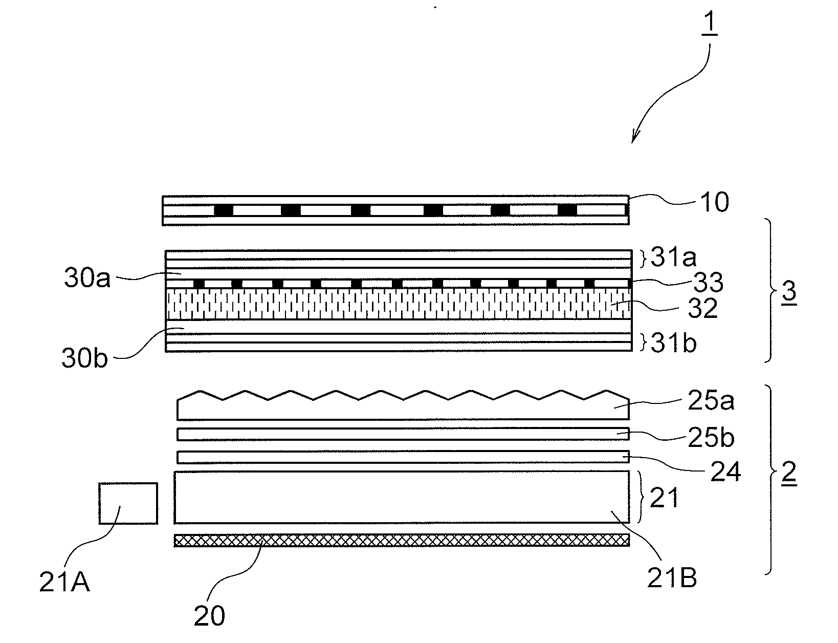
[0033]First, basic contents of a first exemplary embodiment will be described, and the specific contents thereof will be described in details thereafter.

[0034]In FIG. 1 and FIG. 4, an optical writing device 1 according to the first exemplary embodiment includes: a spatial light modulating element 3 which emits image light S towards a display recording medium 4 shown in FIG. 3; a surface-type light source section 2 which feeds, to the spatial light modulating element 3, image forming surface-type light for allowing the spatial light modulating element 3 to emit the image light S; and a surface-type optical element 10 which is mounted on the spatial light modulating element 3 by being opposed to the display recording medium 4 to restrict a spread range of the emission directions of the image light S.

[0035]As shown in FIG. 4, the display recording medium 4 shown in FIG. 3 is arranged by being opposed to the optical element 10 placed on the spatial light modulating element 3. That is, i...

second exemplary embodiment

[0114]Next, an optical writing device according to a second exemplary embodiment of the present invention will be described.

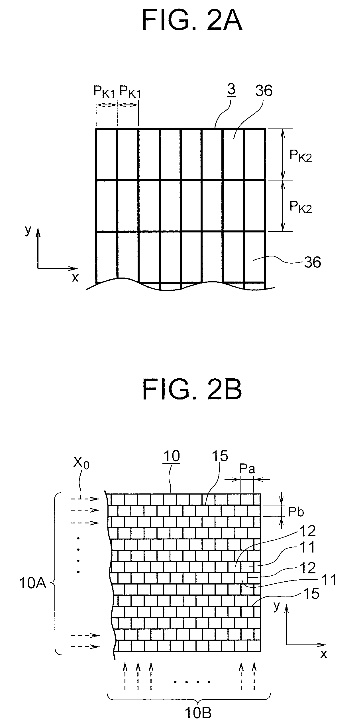
[0115]In the second exemplary embodiment, the periodic structure of the spatial light modulating element 3 loaded to the optical writing device 1 of the first exemplary embodiment described above is in a different structure as shown in FIG. 5.

[0116]As shown in FIG. 5, in the spatial light modulating element 50, the period pitches Pk1 and Pk2 of the repeated periods in the x-direction (direction along the x-axis) and in the y-direction (direction along the y-axis) on the x-y Cartesian coordinates are set to match with each other. A plurality of pixels 51 are spatially arranged in matrix based thereupon to form a periodic structure. The layout of the pixels 51 of the spatial light modulating element 50 shown in FIG. 5 is different from the layout of the pixels 36 of the spatial light modulating element 3 shown in FIG. 3. That is, the length of the long side (Pk2)...


PUM

PropertyMeasurementUnit
widthaaaaaaaaaa
widthaaaaaaaaaa
widthaaaaaaaaaa

Abstract

To provide an optical writing device that outputs image light to be recorded to a display recording medium. An optical element thereof includes a two-dimensional periodic structural body including periodic structure sections sectioned along a direction orthogonal to the direction along which transparent layers and light absorption layers are arranged alternately in a repeated manner. At least a part of the periodic structure sections is in a periodic structure in which the transparent layers and the light absorption layers are arranged alternately by varying phases of spatial frequencies of the transparent layers neighboring in the orthogonal direction. Repeated period pitches of the transparent layers and the light absorption layers in the two orthogonal directions of the two-dimensional periodic structural body are set to match with each other, and the repeated period pitches are set to be narrower than a layout pitch of the pixels of the spatial light modulating element.

Description

CROSS-REFERENCE TO RELATED APPLICATION[0001]This application is based upon and claims the benefit of priority from Japanese patent application No. 2009-237688, filed on Oct. 14, 2009, and Japanese patent application No. 2010-213461, filed on Sep. 24, 2010, the disclosure of which is incorporated herein in its entirety by reference.BACKGROUND OF THE INVENTION[0002]1. Field of the Invention[0003]The present invention relates to an optical writing device. More specifically, the present invention relates to an optical writing device that is capable of writing image information to a display recording medium having a property of memory.[0004]2. Description of the Related Art[0005]Other than a paper medium and an electronic display device as display recording media, a display recording medium having the advantages of both the electronic display and the paper medium has recently been drawing attentions.[0006]Such display recording medium has a property of memory for display. Thus, it is onl...

Claims


Application Information

Patent Timeline
Patent Type & Authority Applications(United States)
IPC IPC(8): G02F1/135
CPCG02F1/133524G02F1/13476G02F2001/1351G02F1/13718G02F2001/13345G02F1/135G02F1/13345G02F1/1351
Inventor MIMURA, KOJI
Owner NEC LCD TECH CORP
Why Eureka
Try Eureka