
Memory and Method of Fabricating the Same

Active Publication Date: 2011-04-21
MACRONIX INT CO LTD
View PDF5 Cites 48 Cited by
  • Summary
  • Abstract
  • Description
  • Claims
  • Application Information

AI Technical Summary

Benefits of technology

[0009]A memory and a method of fabricating the same are described herein. The memory has at least two metal oxide layers. The resistance of the memory equals the sum of the individual resistance of these two metal oxide layers, and a window between the initial resistance and maximum resistance is enlarged. It therefore allows to be applied for the multi-level operation or multi-bits operation. In addition, one or two additional steps will be added to the conventional method of fabricating the memory, as a result of low cost and simple process.
[0010]A memory is provided. The memory element comprises a metal portion, first metal oxide layer and second metal oxide layer. The first metal oxide layer is on the metal element, and the first metal oxide layer includes N resistance levels. The second metal oxide layer is on the first metal oxide layer, and the second metal oxide layer includes M resistance levels. The memory has X resistance levels and X is less than the summation of M and N, for minimizing a programming disturbance.
[0011]A method of fabricating a memory is provided. The method comprises: (a) providing a metal portion; (b) forming a first metal oxide layer on the metal portion, the first metal oxide layer including N resistance levels; and (c) forming a second metal oxide layer on the first metal oxide layer, the second metal oxide layer including M resistance levels, wherein the memory has X resistance levels and X is less than the summation of M and N, for minimizing a programming disturbance.

Problems solved by technology

ROM retains the contents even in the absence of power, but is limited in the speed, the number of times to which it may be written, and the manner in which it may be written.
However, its volatility (i.e. it will lose its contents when the power is switched off), large size and stand-by current limit the total size and applications of the memory.
DRAM has the smallest cell size, but necessitates a complex refresh algorithm, and is also necessary to supply voltage at all times or the information will disappear (i.e. volatile).
More risks caused by complicated steps are also introduced in fabrication.

Method used


Image

  • Memory and Method of Fabricating the Same
  • Memory and Method of Fabricating the Same
  • Memory and Method of Fabricating the Same

Examples


Embodiment Construction

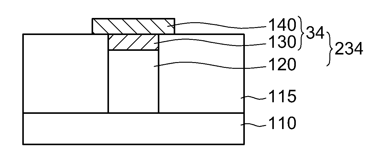
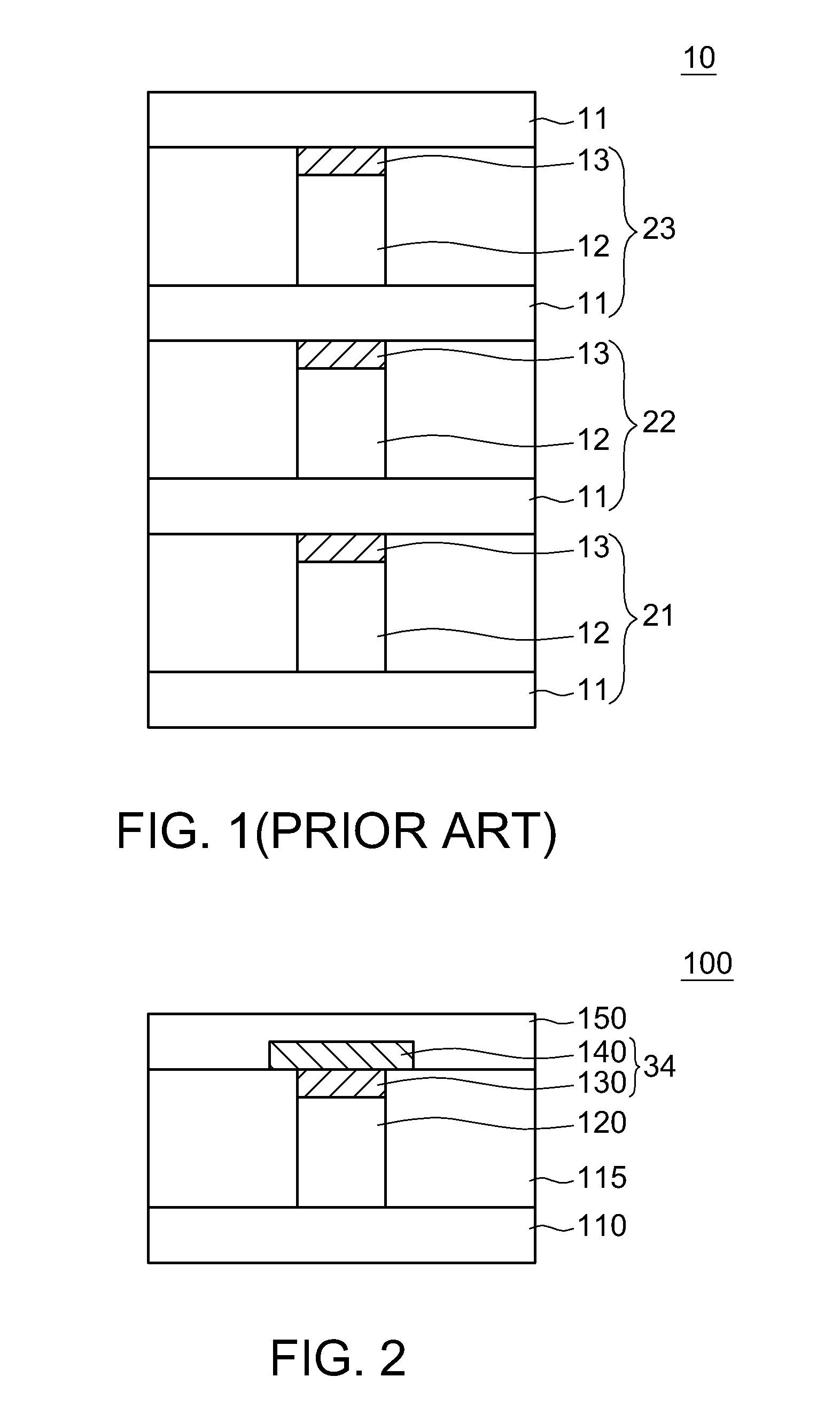
[0021]In the present embodiment, a memory and a method of fabricating the same are disclosed. The memory has two or more metal oxide layers (e.g. first and second metal oxide layers) stacked together. The first metal oxide layer and the second metal oxide layer have an electrical-graded property characterized by a plurality of resistance levels. According to the present embodiment, a structure of the memory capable of applying to multi-level operation or multi-bits operation is disclosed and fabricated by a simple and low-cost method. The embodiments disclosed herein are used for illustrating the invention, but not for limiting the scope of the invention.

[0022]The memory of the present disclosure comprises a metal portion, first metal oxide layer and second metal oxide layer. The first metal oxide layer is formed on the metal element, and the first metal oxide layer includes N resistance levels. The second metal oxide layer is on the first metal oxide layer, and the second metal oxi...


PUM


Abstract

A memory, comprising a metal portion, a first metal layer and second metal oxide layer is provided. The first metal oxide layer is on the metal element, and the first metal oxide layer includes N resistance levels. The second metal oxide layer is on the first metal oxide layer, and the second metal oxide layer includes M resistance levels. The memory has X resistance levels and X is less than the summation of M and N, for minimizing a programming disturbance.

Description

BACKGROUND OF THE INVENTION[0001]1. Field of the Invention[0002]The invention relates in general to a memory and a method of fabricating the same, and more particularly to a memory having two metal oxide layers and a method of fabricating the same.[0003]2. Description of the Related Art[0004]Integrated circuits are used to control the functions of many modern electronic devices. Memory devices used for storing (write) and retrieving (read) data possess advantages that are easily accessible by the integrated circuits. Various types of memory devices for data storage are known in the art. Generally, memory devices are distinguished by their speed and data retention characteristic.[0005]Memory device falls mainly into two classes: random access memory (“RAM”) and read-only memory (“ROM”). Many improvements and variations of RAMs and ROMs have been advanced to further their performance, and both types of memory have their own advantages and disadvantages. Typically, RAM (i.e. volatile) ...

Claims


Application Information

Patent Timeline
IPC IPC(8): H01L45/00H01L29/12H01L21/34
CPCG11C11/5685G11C13/0007H01L45/146H01L45/04H01L45/1233H01L45/1633H10N70/20H10N70/826H10N70/8833H10N70/028
Inventor CHANG, KUO-PINLAI, ERH-KUN
Owner MACRONIX INT CO LTD
Features
  • Generate Ideas
  • Intellectual Property
  • Life Sciences
  • Materials
  • Tech Scout
  • Unparalleled Data Quality
  • Higher Quality Content
  • 60% Fewer Hallucinations
Learn More