

Semiconductor device
a technology of semiconductor devices and semiconductors, applied in semiconductor devices, semiconductor/solid-state device details, electrical devices, etc., can solve the problems of generating heat, fewer advantages of heat dissipation plates and heat propagation lines, and rarely arise heat is not dissipated, so as to improve the yield of semiconductor devices, improve the thermal conductivity, and dissipate heat from an intermediate
- Summary
- Abstract
- Description
- Claims
- Application Information
AI Technical Summary
Benefits of technology
Problems solved by technology
Method used
Image

Examples
first embodiment
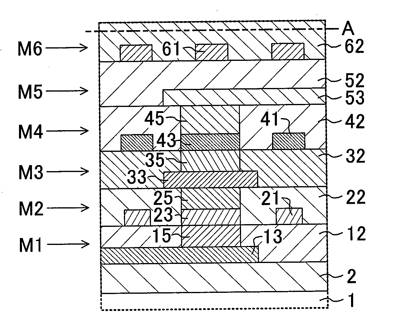
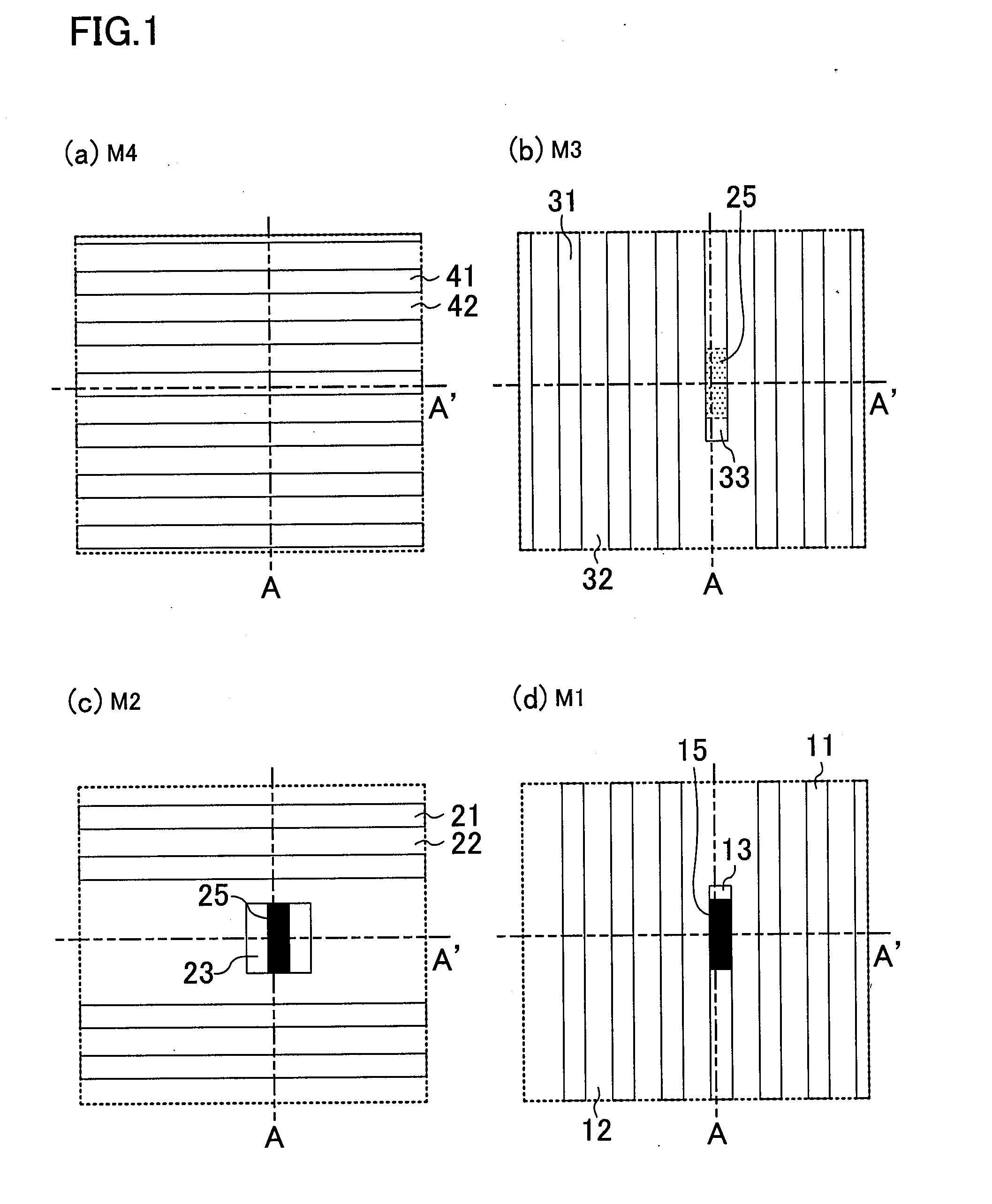
[0026]A semiconductor device according to a first embodiment has a multilayer interconnect structure formed above a substrate. The multilayer interconnect structure includes a first interconnect layer, a second interconnect layer, a third interconnect layer, and a fourth interconnect layer which are stacked from the substrate side in this order.
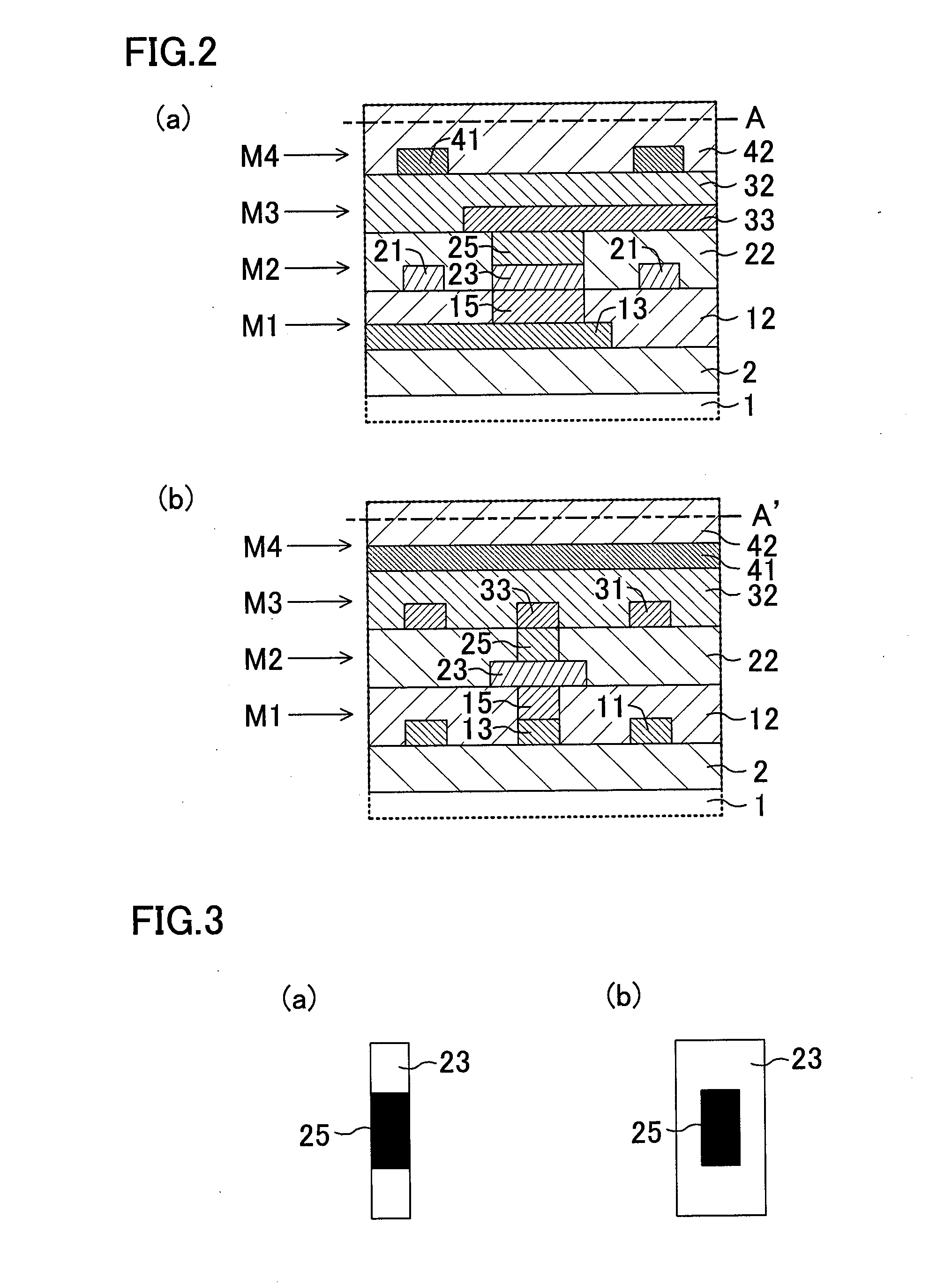
[0027]FIGS. 1A-1D are plan views illustrating a configuration of the semiconductor device according to the present embodiment, wherein FIGS. 1A-1D illustrate configurations of the fourth interconnect layer (M4), the third interconnect layer (M3), the second interconnect layer (M2), and the first interconnect layer (M1), respectively. FIGS. 2A and 2B are cross-sectional views of the semiconductor device of FIGS. 1A-1D, wherein FIG. 2A is a cross-sectional view taken along the line A, and FIG. 2B is a cross-sectional view taken along the line A′.
[0028]In FIGS. 2A and 2B, reference numeral 1 denotes a well region forming a diffusion layer of a t...
second embodiment
[0038]A semiconductor device according to a second embodiment has a configuration almost the same as that of the semiconductor device according to the first embodiment. However, the second embodiment is different from the first embodiment in that in a stack structure of the second embodiment, an intermediate interconnect is not formed, but contact vias are directly connected to each other.
[0039]FIGS. 4A-4D are plan views illustrating a configuration of the semiconductor device according to the present embodiment, wherein FIGS. 4A-4D illustrate configurations of a fourth interconnect layer (M4), a third interconnect layer (M3), a second interconnect layer (M2), and a first interconnect layer (M1), respectively. FIGS. 5A and 5B are cross-sectional views of the semiconductor device of FIGS. 4A-4D, wherein FIG. 5A is a cross-sectional view taken along the line A, and FIG. 5B is a cross-sectional view taken along the line A′. Components in FIGS. 4A-4D, 5A, and 5B which are substantially ...
third embodiment
[0046]In a semiconductor device according to a third embodiment, a multilayer interconnect structure formed above a substrate includes a first interconnect layer, a second interconnect layer, a third interconnect layer, a fourth interconnect layer, and a fifth interconnect layer which are stacked from the substrate in this order.
[0047]FIGS. 6A-6E are plan views illustrating a configuration of the semiconductor device according to the present embodiment, wherein FIGS. 6A-6E illustrate configurations of the fifth interconnect layer (M5), the fourth interconnect layer (M4), the third interconnect layer (M3), the second interconnect layer (M2), and the first interconnect layer (M1), respectively. FIGS. 7A and 7B are cross-sectional views of the semiconductor device of FIGS. 6A-6E, wherein FIG. 7A is a cross-sectional view taken along the line A, and FIG. 7B is a cross-sectional view taken along the line A′.
[0048]In FIGS. 7A and 7B, reference numeral 1 denotes a well region forming a dif...
PUM
 Abstract
Description
Claims
Application Information