

Imaging device, method for controlling imaging device and program product
a technology of imaging device and program product, which is applied in the direction of exposure control, color signal processing circuit, instruments, etc., can solve the problems of affecting the stability of exposure control, and unable to obtain appropriate exposure without execution of these processing, so as to improve the stability performance of exposure control and stabilize the control faster
- Summary
- Abstract
- Description
- Claims
- Application Information
AI Technical Summary
Benefits of technology
Problems solved by technology
Method used
Image

Examples
first exemplary embodiment
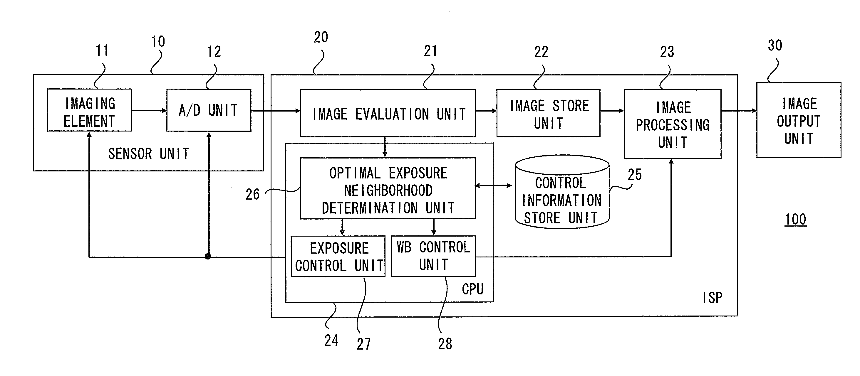
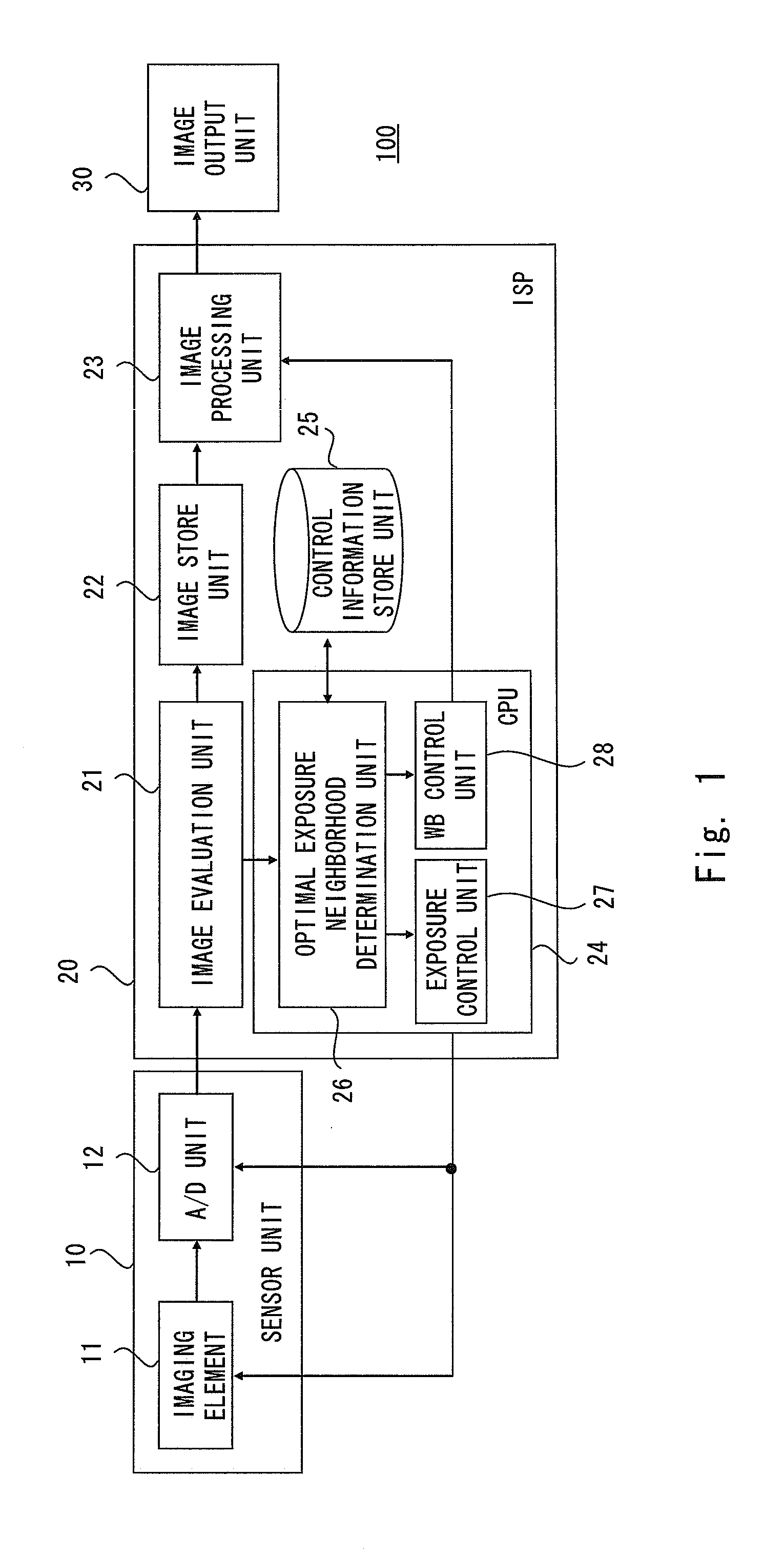
[0031]FIG. 1 is a view showing an imaging device of the first exemplary embodiment. An imaging device 100 includes an imaging sensor unit 10, an imaging sensor processing unit 20 (hereinafter referred to as “ISP” (Image Sensor Processor)), and an image output unit 30.
[0032]The imaging sensor unit 10 includes CCD or CMOS and so on, and further includes an imaging element 11 which obtains an image, and an analog-digital converter (A / D unit) 12 which converts an image obtained by the imaging element 11 from an analog signal into a digital signal. The ISP 20 includes an image evaluation unit 21, an image store unit 22, an image processing unit 23, a CPU 24, and a control information store unit 25, and the CPU 24 includes an optimal exposure neighborhood determination unit 26, an exposure control unit 27, and a white balance control unit (WB control unit) 28.
[0033]The image evaluation unit 21 calculates a luminance value of an image data obtained by the imaging element 11. The CPU 24 cal...
second exemplary embodiment
[0057]Next, a second exemplary embodiment will be explained. In the above first exemplary embodiment, three initial values for the exposure with which the defensive ranges are set not to overlap each other are used. On the other hand, in the present exemplary embodiment, a setting sequence of three initial values for the exposure is specified. This can stabilize the white balance controlling with faster speed. The constitution of the imaging device 100 is the same as that in the first exemplary embodiment shown in FIG. 1.
[0058]FIG. 7 is a view to explain the initial values for the exposure of the present exemplary embodiment. In the first exemplary embodiment, although the initial values for the exposures with which the defensive ranges are set not to overlap each other are used, the sequence is not specified. On the other hand, in the present exemplary embodiment, an initial value for the exposure set in the first frame (a first initial value) is a setting value which can obtain an...
PUM
 Abstract
Description
Claims
Application Information