Fault protector for opto-electronic devices and associated methods

a technology of opto-electronic devices and fault protectors, applied in the direction of emergency protective circuit arrangements, limiting excess voltage/current, semiconductor lasers, etc., can solve the problems of opto-electronic device failure, product containing opto-electronic devices often seem to mysteriously fail, and easy damage to most opto-electronic devices, so as to avoid adding significant resistance or capacitance to the laser diode, and not complicating the task of driving

Active Publication Date: 2011-05-12
BENNER JR WILLIAM R
View PDF13 Cites 8 Cited by
  • Summary
  • Abstract
  • Description
  • Claims
  • Application Information

AI Technical Summary

Benefits of technology

The device described in this patent prevents the voltage from damaging the laser diode and avoids other power-related issues. This is done without adding any resistance or capacitance to the laser diode, making it easier to drive.

Problems solved by technology

The technical problem addressed in this patent text is finding an effective way to protect low-power laser diodes from electrostatic discharge (ESD) events without using a relay or a depletion-mode MOSFET. The impedance of a capacitor or a simple resistor in series with the laser diode is too high, and a multi-layer varistor would not be fast enough to protect against a 15,000-volt ESD event. The "switch" approach using a relay or depletion-mode MOSFET has its limitations, such as contact resistance and interconnect resistance. The "switch" approach also has the drawback of conducting ESD through the system power-off, which can damage the laser diode. A new approach is needed to protect low-powered laser diodes from ESD events.

Method used


Image

  • Fault protector for opto-electronic devices and associated methods
  • Fault protector for opto-electronic devices and associated methods
  • Fault protector for opto-electronic devices and associated methods

Examples


Embodiment Construction

[0051]The present invention will now be described more fully hereinafter with reference to the accompanying drawings, in which preferred embodiments of the invention are shown. This invention may, however, be embodied in many different forms and should not be construed as limited to the embodiments set forth herein. Rather, these embodiments are provided so that this disclosure will be thorough and complete, and will fully convey the scope of the invention to those skilled in the art.

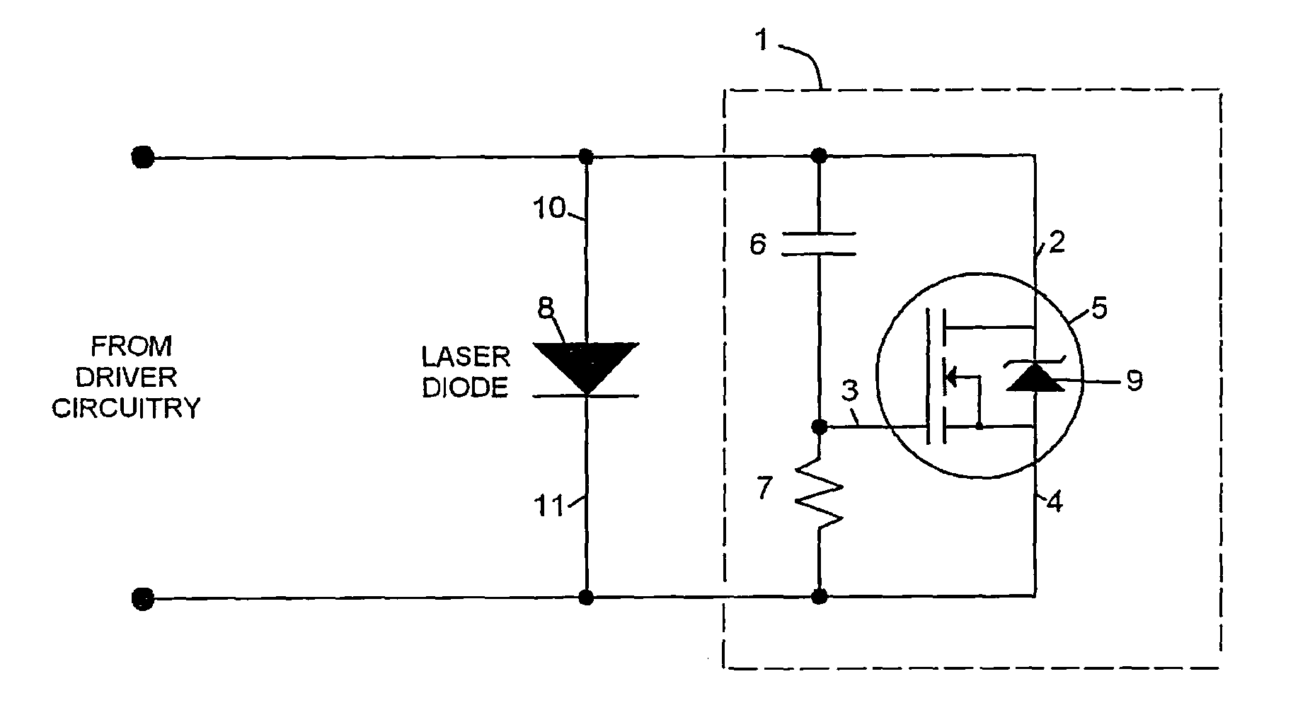
[0052]One embodiment of the invention, as illustrated with reference to FIG. 9, is described in the context of its use to protect a laser diode from ESD and other power-related faults. One of skill in the art will recognize that the device of the present invention can be used with other opto-electronic elements, and that this usage is not intended as a limitation. The device relies on a few passive components, and a class of enhancement-mode MOSFETs that have a very low gate-to-source threshold voltage ...


PUM


Abstract

A fault protector for an opto-electronic device includes a MOSFET having an integral body-diode. A capacitor is connected between a drain and a gate of the MOSFET, and a resistor is connected between the gate and a source of the MOSFET. The drain of the MOSFET is connectable to a first terminal of an opto-electronic device, and the source of the MOSFET is connectable to a second terminal of the opto-electronic device. The device overcomes problems of previously known techniques by preventing a reverse-bias voltage from exceeding an absolute maximum specified by a manufacturer, and also prevents ESD or other power-related faults from exceeding the maximum forward-bias voltage of the laser diode, while not adding significant resistance or capacitance to the laser diode, thereby not complicating the task of driving the laser diode.

Description


Claims


Application Information

Patent Timeline
Owner BENNER JR WILLIAM R
Why Eureka
Try Eureka