Method for manufacturing liquid crystal display device

a technology of liquid crystal display and liquid crystal, which is applied in the direction of semiconductor devices, basic electric elements, electrical appliances, etc., can solve the problems of requiring a lot of labor and time, and achieve the effect of shortening the photolithography process

Inactive Publication Date: 2011-05-12
PANASONIC LIQUID CRYSTAL DISPLAY CO LTD +1
View PDF7 Cites 20 Cited by
  • Summary
  • Abstract
  • Description
  • Claims
  • Application Information

AI Technical Summary

Benefits of technology

[0008]The present invention aims to shorten the p...

Problems solved by technology

The etching resist is patterned by photolithogr...

Method used


Image

  • Method for manufacturing liquid crystal display device
  • Method for manufacturing liquid crystal display device
  • Method for manufacturing liquid crystal display device

Examples


Embodiment Construction

[0030]Hereinafter, the embodiment of the present invention will be described with reference to the drawings.

[Liquid Crystal Display Device]

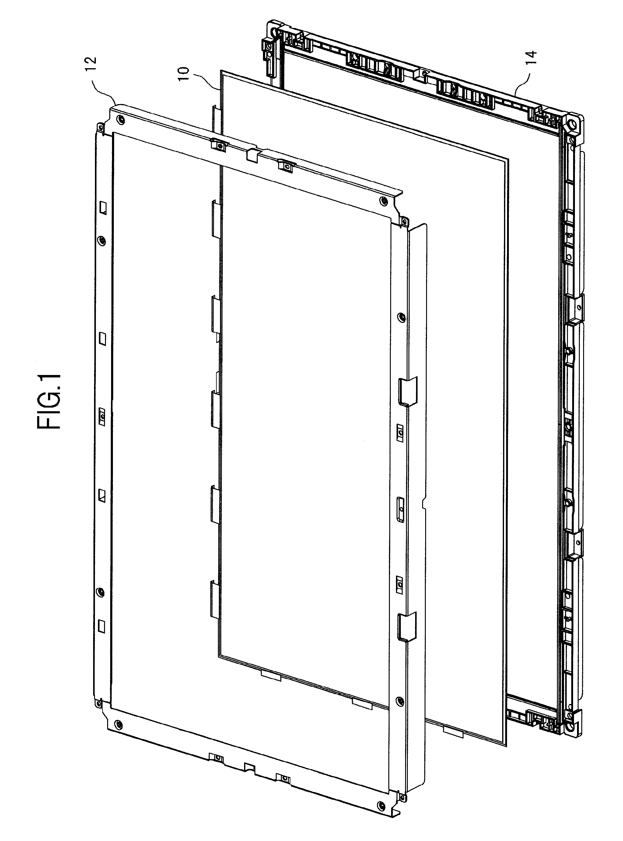
[0031]FIG. 1 is an exploded perspective view showing a liquid crystal display device according to an embodiment of the present invention. The liquid crystal display device includes a liquid crystal display panel 10. The liquid crystal display panel 10 is supported by an upper frame 12 and a lower frame 14.

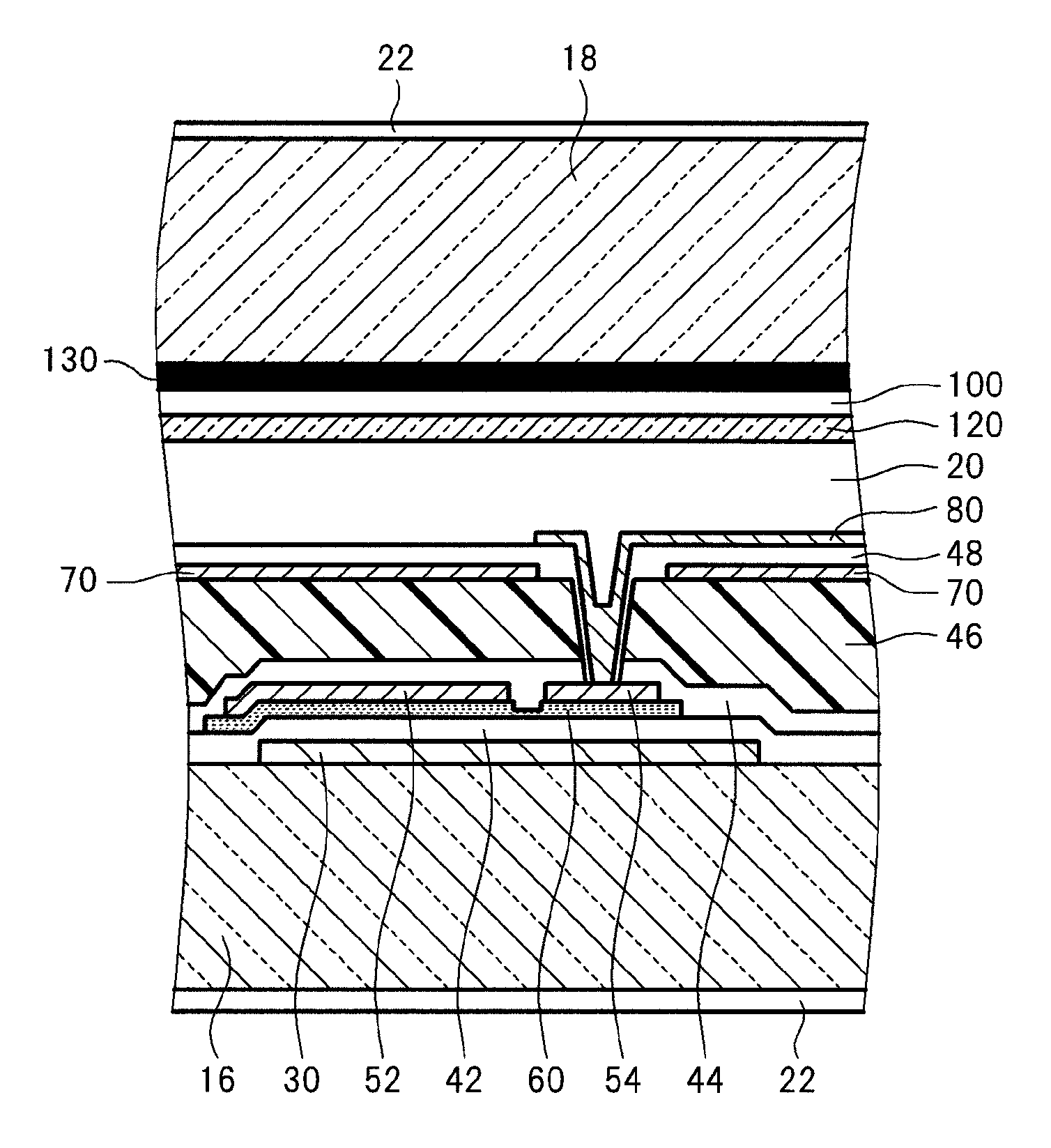
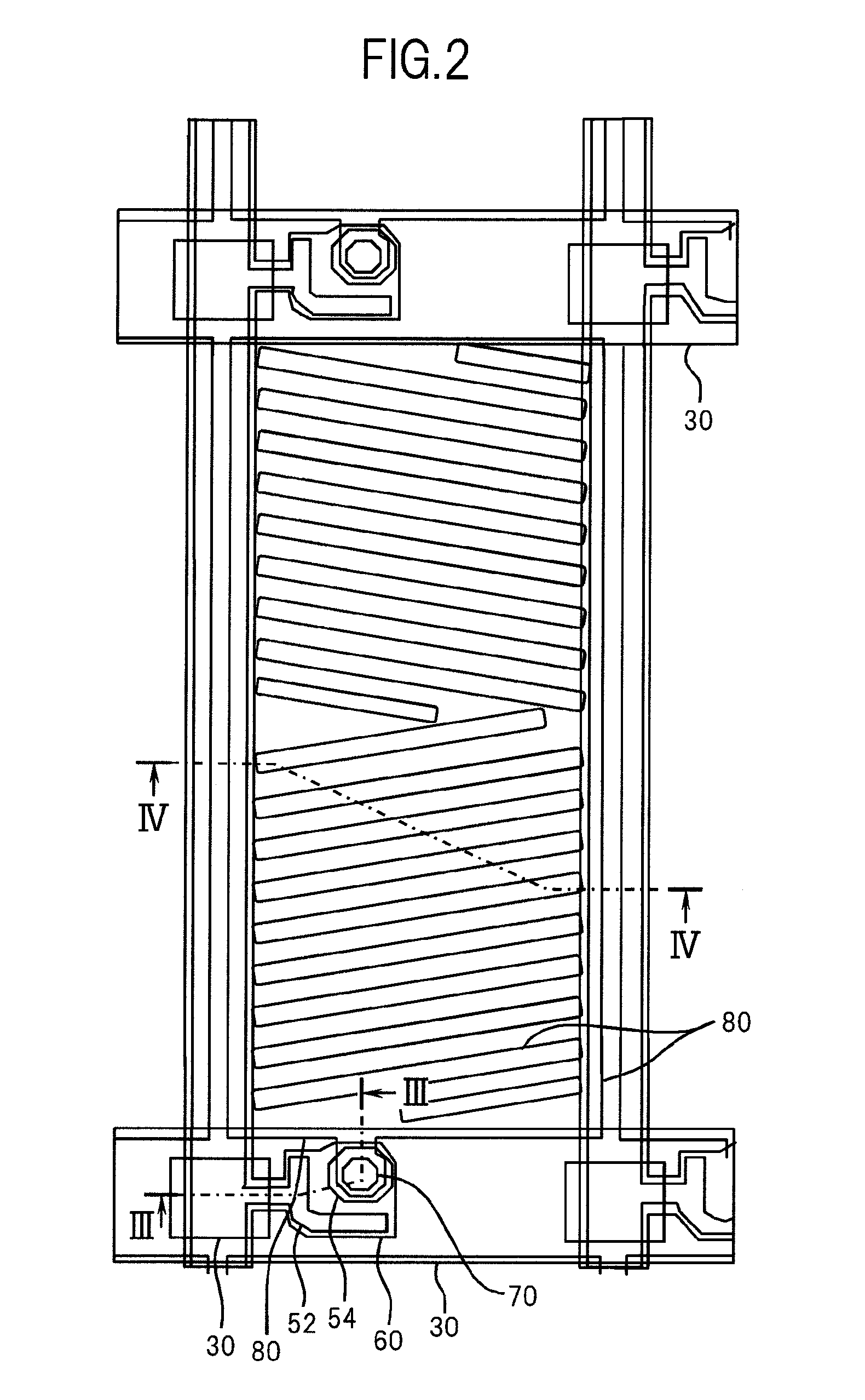
[0032]FIG. 2 is a schematic top view showing a portion of the liquid crystal display panel 10 of the liquid crystal display device shown in FIG. 1. FIG. 3 is a sectional view of the liquid crystal display panel 10 taken along the line in FIG. 2. FIG. 4 is a sectional view of the liquid crystal display panel 10 taken along the line IV-IV in FIG. 2

[0033]The structure of the liquid crystal display panel 10 is illustrated using the sectional view of FIG. 3. The liquid crystal display panel 10 includes a first substrate 16 and a second substrate 18 (...


PUM


Abstract

A thin-film transistor including a gate electrode, a drain electrode, and a source electrode is formed. A first insulating film is formed so as to cover the thin-film transistor. A second insulating film is formed on the first insulating film. A transparent conductive film is formed on the second insulating film. An etching resist which is patterned by a photolithography process is formed on the transparent conductive film. A first transparent electrode is formed by patterning the transparent conductive film by a first etching using the etching resist. A penetration hole is formed in the second insulating film at a position above one of the drain electrode and the source electrode by a second etching which is performed using the etching resist on a surface of the second insulating film exposed from the first transparent electrode.

Description

CROSS-REFERENCE TO RELATED APPLICATION[0001]The present application claims priority from Japanese application JP2009-255699 filed on Nov. 9, 2009, the content of which is hereby incorporated by reference into this application.BACKGROUND OF THE INVENTION[0002]1. Field of the Invention[0003]The present invention relates to a method for manufacturing a liquid crystal display device.[0004]2. Description of the Related Art[0005]Liquid crystal display devices have a TFT substrate in which thin-film transistors (TFT) for driving liquid crystals are formed and a color filter substrate in which color filters are formed, and liquid crystals are interposed between the two substrates. In such liquid crystal display devices, a liquid crystal display device which displays images by applying a transverse electric field to the liquid crystals is referred to as an In-Plane Switching (IPS)-mode liquid crystal display device. Such a liquid crystal display device is known to have a wide viewing field a...

Claims


Application Information

Patent Timeline
IPC IPC(8): H01L21/306
CPCH01L27/1288H01L27/124
Inventor ONO, KIKUO
Owner PANASONIC LIQUID CRYSTAL DISPLAY CO LTD
Why Eureka
Try Eureka